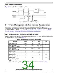
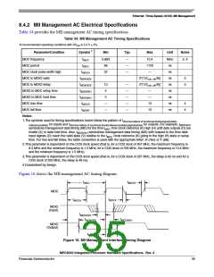
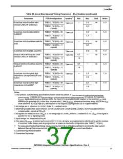
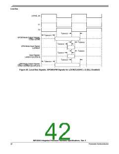
Local Bus
Table 37 describes the general timing parameters of the local bus interface of the MPC8540 with the DLL
bypassed.
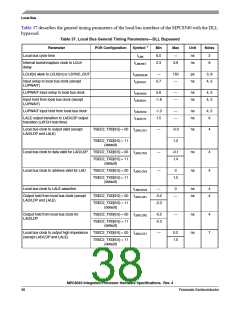
Table 37. Local Bus General Timing Parameters—DLL Bypassed
Parameter
Local bus cycle time
POR Configuration
Symbol 1
Min
Max
Unit
Notes
tLBK
6.0
2.3
—
ns
ns
2
8
Internal launch/capture clock to LCLK
delay
tLBKHKT
3.9
LCLK[n] skew to LCLK[m] or LSYNC_OUT
tLBKSKEW
tLBIVKH1
—
150
—
ps
ns
3, 9
4, 5
Input setup to local bus clock (except
LUPWAIT)
5.7
LUPWAIT input setup to local bus clock
tLBIVKH2
tLBIXKH1
5.6
—
—
ns
ns
4, 5
4, 5
Input hold from local bus clock (except
LUPWAIT)
-1.8
LUPWAIT input hold from local bus clock
tLBIXKH2
tLBOTOT
-1.3
1.5
—
—
ns
ns
4, 5
6
LALE output transition to LAD/LDP output
transition (LATCH hold time)
Local bus clock to output valid (except
LAD/LDP and LALE)
TSEC2_TXD[6:5] = 00
tLBKLOV1
—
-0.3
1.2
ns
4
TSEC2_TXD[6:5] = 11
(default)
Local bus clock to data valid for LAD/LDP
Local bus clock to address valid for LAD
Local bus clock to LALE assertion
TSEC2_TXD[6:5] = 00
tLBKLOV2
—
—
-0.1
1.4
ns
ns
4
4
TSEC2_TXD[6:5] = 11
(default)
TSEC2_TXD[6:5] = 00
tLBKLOV3
0
TSEC2_TXD[6:5] = 11
(default)
1.5
tLBKHOV4
tLBKLOX1
—
0
ns
ns
4
4
Output hold from local bus clock (except
LAD/LDP and LALE)
TSEC2_TXD[6:5] = 00
-3.2
-2.3
—
TSEC2_TXD[6:5] = 11
(default)
Output hold from local bus clock for
LAD/LDP
TSEC2_TXD[6:5] = 00
tLBKLOX2
-3.2
-2.3
—
ns
ns
4
7
TSEC2_TXD[6:5] = 11
(default)
Local bus clock to output high Impedance TSEC2_TXD[6:5] = 00
(except LAD/LDP and LALE)
tLBKLOZ1
—
0.2
1.5
TSEC2_TXD[6:5] = 11
(default)
MPC8540 Integrated Processor Hardware Specifications, Rev. 4
38
Freescale Semiconductor

 FREESCALE [ Freescale ]