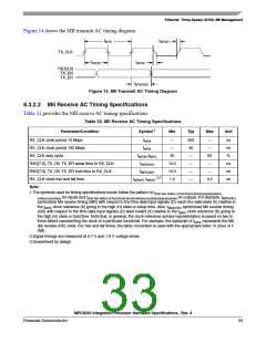
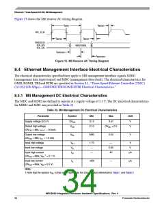
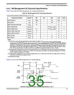
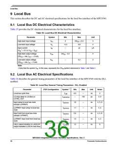
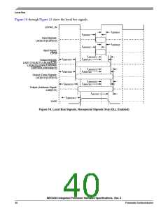
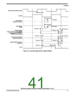
Local Bus
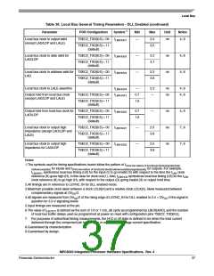
Table 36. Local Bus General Timing Parameters - DLL Enabled (continued)
Parameter
POR Configuration
Symbol 1
Min
Max
Unit
Notes
Local bus clock to output valid
(except LAD/LDP and LALE)
TSEC2_TXD[6:5] = 00
tLBKHOV1
—
2.0
3.5
ns
4, 8
4, 8
4, 8
TSEC2_TXD[6:5] = 11
(default)
Local bus clock to data valid for
LAD/LDP
TSEC2_TXD[6:5] = 00
tLBKHOV2
—
—
2.2
3.7
ns
ns
TSEC2_TXD[6:5] = 11
(default)
Local bus clock to address valid for TSEC2_TXD[6:5] = 00
LAD
tLBKHOV3
2.3
3.8
TSEC2_TXD[6:5] = 11
(default)
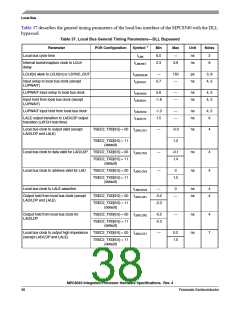
Local bus clock to LALE assertion
tLBKHOV4
tLBKHOX1
—
2.3
—
ns
ns
4, 8
4, 8
Output hold from local bus clock
(except LAD/LDP and LALE)
TSEC2_TXD[6:5] = 00
0.7
1.6
TSEC2_TXD[6:5] = 11
(default)
Output hold from local bus clock for TSEC2_TXD[6:5] = 00
tLBKHOX2
tLBKHOZ1
tLBKHOZ2
0.7
1.6
—
ns
ns
ns
4, 8
7, 9
7, 9
LAD/LDP
TSEC2_TXD[6:5] = 11
(default)
Local bus clock to output high
Impedance (except LAD/LDP and
LALE)
TSEC2_TXD[6:5] = 00
—
—
2.5
3.8
TSEC2_TXD[6:5] = 11
(default)
Local bus clock to output high
impedance for LAD/LDP
TSEC2_TXD[6:5] = 00
2.5
3.8
TSEC2_TXD[6:5] = 11
(default)
Notes:
1.The symbols used for timing specifications herein follow the pattern of t(First two letters of functional block)(signal)(state)
(reference)(state) for inputs and t(First two letters of functional block)(reference)(state)(signal)(state) for outputs. For example,
tLBIXKH1 symbolizes local bus timing (LB) for the input (I) to go invalid (X) with respect to the time the tLBK clock
reference (K) goes high (H), in this case for clock one(1). Also, tLBKHOX symbolizes local bus timing (LB) for the tLBK
clock reference (K) to go high (H), with respect to the output (O) going invalid (X) or output hold time.
2.All timings are in reference to LSYNC_IN for DLL enabled mode.
3.Maximum possible clock skew between a clock LCLK[m] and a relative clock LCLK[n]. Skew measured between
complementary signals at OVDD/2.
4.All signals are measured from OVDD/2 of the rising edge of LSYNC_IN for DLL enabled to 0.4 × OVDD of the signal in
question for 3.3-V signaling levels.
5.Input timings are measured at the pin.
6.The value of tLBOTOT is defined as the sum of 1/2 or 1 ccb_clk cycle as programmed by LBCR[AHD], and the number
of local bus buffer delays used as programmed at power-on reset with configuration pins TSEC2_TXD[6:5].
7. For purposes of active/float timing measurements, the Hi-Z or off state is defined to be when the total current
delivered through the component pin is less than or equal to the leakage current specification.
8.Guaranteed by characterization.
9.Guaranteed by design.
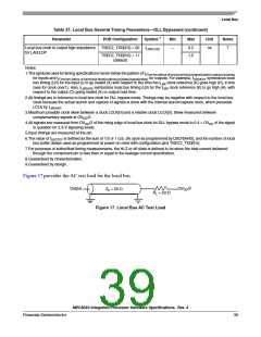
MPC8540 Integrated Processor Hardware Specifications, Rev. 4
Freescale Semiconductor
37

 FREESCALE [ Freescale ]