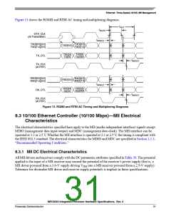
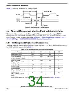
Ethernet: Three-Speed,10/100, MII Management
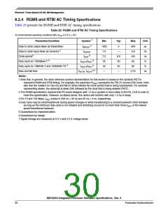
8.2.4 RGMII and RTBI AC Timing Specifications
Table 29 presents the RGMII and RTBI AC timing specifications.
Table 29. RGMII and RTBI AC Timing Specifications
At recommended operating conditions with LVDD of 2.5 V 5%.
Parameter/Condition
Symbol 1
Min
Typ
Max
Unit
5
Data to clock output skew (at transmitter)
Data to clock input skew (at receiver) 2
Clock period3
tSKRGT
–500
1.0
7.2
45
0
500
2.8
8.8
55
ps
ns
ns
%
tSKRGT
—
8.0
50
50
—
6
tRGT
Duty cycle for 1000Base-T 4
Duty cycle for 10BASE-T and 100BASE-TX 3
Rise and fall time
tRGTH/tRGT
6
6
tRGTH/tRGT
40
60
%
6,7
tRGTR, tRGTF
—
0.75
ns
Notes:
1.Note that, in general, the clock reference symbol representation for this section is based on the symbols RGT to
represent RGMII and RTBI timing. For example, the subscript of tRGT represents the TBI (T) receive (RX) clock. Note
also that the notation for rise (R) and fall (F) times follows the clock symbol that is being represented. For symbols
representing skews, the subscript is skew (SK) followed by the clock that is being skewed (RGT).
2.The RGMII specification requires that PC board designer add 1.5 ns or greater in trace delay to the RX_CLK in order to
meet this specification. However, as stated above, this device will function with only 1.0 ns of delay.
3.For 10 and 100 Mbps, tRGT scales to 400 ns 40 ns and 40 ns 4 ns, respectively.
4.Duty cycle may be stretched/shrunk during speed changes or while transitioning to a received packet's clock domains
as long as the minimum duty cycle is not violated and stretching occurs for no more than three tRGT of the lowest
speed transitioned between.
5.Guaranteed by characterization.
6.Guaranteed by design.
7.Signal timings are measured at 0.5 V and 2.0 V voltage levels.
MPC8540 Integrated Processor Hardware Specifications, Rev. 4
30
Freescale Semiconductor

 FREESCALE [ Freescale ]