Ethernet: Three-Speed,10/100, MII Management
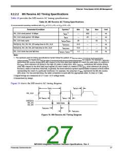
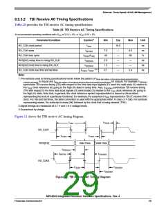
8.2.3.2 TBI Receive AC Timing Specifications
Table 28 provides the TBI receive AC timing specifications.
Table 28. TBI Receive AC Timing Specifications
At recommended operating conditions with LVDD of 3.3 V 5%, or LVDD=2.5V 5%.
Parameter/Condition
RX_CLK clock period
Symbol 1
Min
Typ
Max
Unit
tTRX
16.0
—
ns
ns
%
RX_CLK skew
tSKTRX
7.5
40
8.5
60
—
RX_CLK duty cycle
tTRXH/tTRX
tTRDVKH
tTRDXKH
—
RCG[9:0] setup time to rising RX_CLK
RCG[9:0] hold time to rising RX_CLK
RX_CLK clock rise time and fall time
Note:
2.5
1.5
0.7
—
ns
ns
ns
—
—
2,3
tTRXR, tTRXF
—
2.4
1.The symbols used for timing specifications herein follow the pattern of t(first two letters of functional block)(signal)(state)
(reference)(state) for inputs and t(first two letters of functional block)(reference)(state)(signal)(state) for outputs. For example, tTRDVKH
symbolizes TBI receive timing (TR) with respect to the time data input signals (D) reach the valid state (V) relative to
the tTRX clock reference (K) going to the high (H) state or setup time. Also, tTRDXKH symbolizes TBI receive timing
(TR) with respect to the time data input signals (D) went invalid (X) relative to the tTRX clock reference (K) going to
the high (H) state. Note that, in general, the clock reference symbol representation is based on three letters
representing the clock of a particular functional. For example, the subscript of tTRX represents the TBI (T) receive (RX)
clock. For rise and fall times, the latter convention is used with the appropriate letter: R (rise) or F (fall). For symbols
representing skews, the subscript is skew (SK) followed by the clock that is being skewed (TRX).
2.Signal timings are measured at 0.7 V and 1.9 V voltage levels.
3.Guaranteed by design.
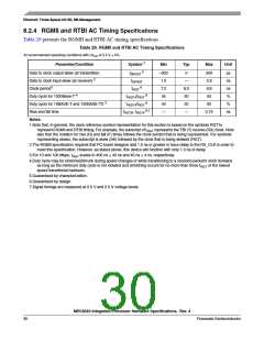
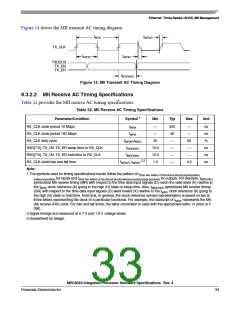
Figure 12 shows the TBI receive AC timing diagram.
tTRXR
tTRX
RX_CLK1
RCG[9:0]
tTRXH
tTRXF
Valid Data
Valid Data
tTRDVKH
tSKTRX
tTRDXKH
RX_CLK0
tTRXH
tTRDXKH
tTRDVKH
Figure 12. TBI Receive AC Timing Diagram
MPC8540 Integrated Processor Hardware Specifications, Rev. 4
Freescale Semiconductor
29

 FREESCALE [ Freescale ]