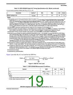
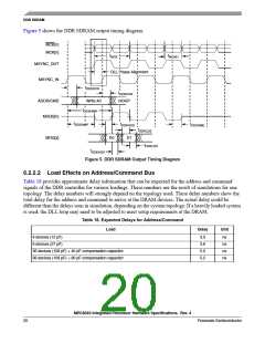
Ethernet: Three-Speed,10/100, MII Management
Table 22. GMII, MII, RGMII, RTBI, and TBI DC Electrical Characteristics
Parameters
Symbol
Min
Max
Unit
Supply voltage 2.5 V
LVDD
VOH
2.37
2.00
2.63
V
V
Output high voltage
LVDD + 0.3
(LVDD = Min, IOH = –1.0 mA)
Output low voltage
VOL
GND – 0.3
0.40
V
(LVDD = Min, IOL = 1.0 mA)
Input high voltage
Input low voltage
Input high current
VIH
VIL
IIH
1.70
–0.3
—
LVDD + 0.3
0.70
V
V
10
μA
(VIN 1 = LVDD
)
Input low current
(VIN 1 = GND)
IIL
–15
—
μA
Note:
1.Note that the symbol VIN, in this case, represents the LVIN symbol referenced in Table 1and Table 2.
8.2 GMII, MII, TBI, RGMII, and RTBI AC Timing Specifications
The AC timing specifications for GMII, MII, TBI, RGMII, and RTBI are presented in this section.
8.2.1 GMII AC Timing Specifications
This section describes the GMII transmit and receive AC timing specifications.
8.2.1.1 GMII Transmit AC Timing Specifications
Table 23 provides the GMII transmit AC timing specifications.
Table 23. GMII Transmit AC Timing Specifications
At recommended operating conditions with LVDD of 3.3 V 5%, or LVDD=2.5V 5%.
Parameter/Condition
GTX_CLK clock period
Symbol 1
Min
Typ
Max
Unit
tGTX
—
40
8.0
—
—
—
—
60
—
ns
%
GTX_CLK duty cycle
tGTXH/tGTX
tGTKHDV
GMII data TXD[7:0], TX_ER, TX_EN setup time
GTX_CLK to GMII data TXD[7:0], TX_ER, TX_EN delay
2.5
0.5
ns
ns
3
tGTKHDX
5.0
MPC8540 Integrated Processor Hardware Specifications, Rev. 4
Freescale Semiconductor
23

 FREESCALE [ Freescale ]