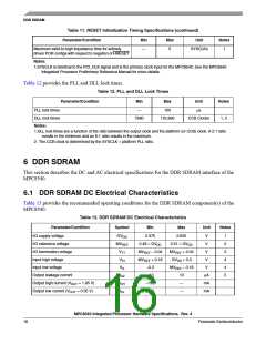
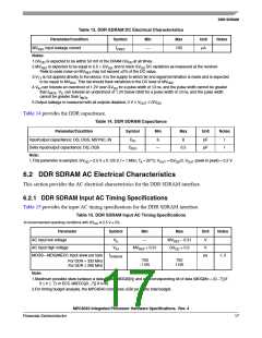
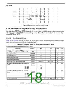
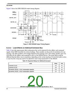
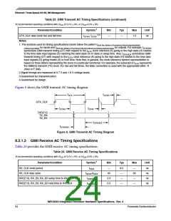
DDR SDRAM
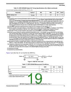
Figure 5 shows the DDR SDRAM output timing diagram.
MCK[n]
MCK[n]
tMtMCCKK
tMCKH
MSYNC_OUT
DLL Phase Alignment
MSYNC_IN
tDDKHOV
tDDKHOX
ADDR/CMD
MDQS[n]
Write A0
tDDSHMH
NOOP
tDDSHMP
tDDKHDS
tDDSHME
tDDKLDS
MDQ[x]
D0
D1
tDDKLDX
tDDKHDX
Figure 5. DDR SDRAM Output Timing Diagram
6.2.2.2 Load Effects on Address/Command Bus
Table 18 provides approximate delay information that can be expected for the address and command
signals of the DDR controller for various loadings. These numbers are the result of simulations for one
topology. The delay numbers will strongly depend on the topology used. These delay numbers show the
total delay for the address and command to arrive at the DRAM devices. The actual delay could be
different than the delays seen in simulation, depending on the system topology. If a heavily loaded system
is used, the DLL loop may need to be adjusted to meet setup requirements at the DRAM.
Table 18. Expected Delays for Address/Command
Load
Delay
Unit
4 devices (12 pF)
9 devices (27 pF)
3.0
3.6
5.0
5.2
ns
ns
ns
ns
36 devices (108 pF) + 40 pF compensation capacitor
36 devices (108 pF) + 80 pF compensation capacitor
MPC8540 Integrated Processor Hardware Specifications, Rev. 4
20
Freescale Semiconductor

 FREESCALE [ Freescale ]