Ethernet: Three-Speed,10/100, MII Management
8 Ethernet: Three-Speed,10/100, MII Management
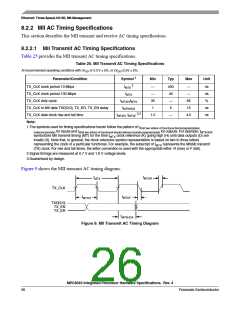
This section provides the AC and DC electrical characteristics for three-speed, 10/100, and MII
management.
8.1 Three-Speed Ethernet Controller (TSEC)
(10/100/1Gb Mbps)—GMII/MII/TBI/RGMII/RTBI Electrical
Characteristics
The electrical characteristics specified here apply to all GMII (gigabit media independent interface), MII
(media independent interface), TBI (ten-bit interface), RGMII (reduced gigabit media independent
interface), and RTBI (reduced ten-bit interface) signals except MDIO (management data input/output) and
MDC (management data clock). The RGMII and RTBI interfaces are defined for 2.5 V, while the GMII,
MII, and TBI interfaces can be operated at 3.3 or 2.5 V. Whether the GMII, MII, or TBI interface is
operated at 3.3 or 2.5 V, the timing is compliant with the IEEE 802.3 standard. The RGMII and RTBI
interfaces follow the Hewlett-Packard reduced pin-count interface for Gigabit Ethernet Physical Layer
Device Specification Version 1.2a (9/22/2000). The electrical characteristics for MDIO and MDC are
specified in Section 8.4, “Ethernet Management Interface Electrical Characteristics.”
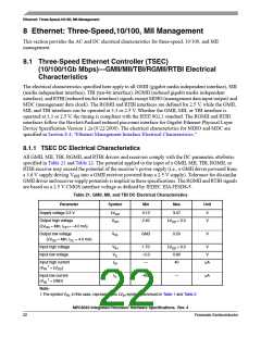
8.1.1 TSEC DC Electrical Characteristics
All GMII, MII, TBI, RGMII, and RTBI drivers and receivers comply with the DC parametric attributes
specified in Table 21 and Table 22. The potential applied to the input of a GMII, MII, TBI, RGMII, or
RTBI receiver may exceed the potential of the receiver’s power supply (i.e., a GMII driver powered from
a 3.6 V supply driving V into a GMII receiver powered from a 2.5 V supply). Tolerance for dissimilar
OH
GMII driver and receiver supply potentials is implicit in these specifications. The RGMII and RTBI signals
are based on a 2.5 V CMOS interface voltage as defined by JEDEC EIA/JESD8-5.
Table 21. GMII, MII, and TBI DC Electrical Characteristics
Parameter
Symbol
Min
Max
Unit
Supply voltage 3.3 V
LVDD
VOH
3.13
2.40
3.47
V
V
Output high voltage
LVDD + 0.3
(LVDD = Min, IOH = –4.0 mA)
Output low voltage
VOL
GND
0.50
V
(LVDD = Min, IOL = 4.0 mA)
Input high voltage
Input low voltage
Input high current
VIH
VIL
IIH
1.70
–0.3
—
LVDD + 0.3
0.90
V
V
40
μA
(VIN 1 = LVDD
)
Input low current
(VIN 1 = GND)
IIL
–600
—
μA
Note:
1.The symbol VIN, in this case, represents the LVIN symbol referenced in Table 1 and Table 2.
MPC8540 Integrated Processor Hardware Specifications, Rev. 4
22
Freescale Semiconductor

 FREESCALE [ Freescale ]