DDR SDRAM
Table 16. DDR SDRAM Output AC Timing Specifications–DLL Mode (continued)
At recommended operating conditions with GVDD of 2.5 V 5%.
Parameter
Symbol 1
tDDSHME
Min
Max
Unit
Notes
MDQS epilogue end
1.5
4.0
ns
7, 8
Notes:
1.The symbols used for timing specifications follow the pattern of t(first two letters of functional block)(signal)(state) (reference)(state) for
inputs and t(first two letters of functional block)(reference)(state)(signal)(state) for outputs. Output hold time can be read as DDR
timing (DD) from the rising or falling edge of the reference clock (KH or KL) until the output went invalid (OX or DX). For
example, tDDKHOV symbolizes DDR timing (DD) for the time tMCK memory clock reference (K) goes from the high (H)
state until outputs (O) are valid (V) or output valid time. Also, tDDKLDX symbolizes DDR timing (DD) for the time tMCK
memory clock reference (K) goes low (L) until data outputs (D) are invalid (X) or data output hold time.
2.All MCK/MCK referenced measurements are made from the crossing of the two signals 0.1 V.
3.Maximum possible clock skew between a clock MCK[n] and its relative inverse clock MCK[n], or between a clock MCK[n]
and a relative clock MCK[m] or MSYNC_OUT. Skew measured between complementary signals at GVDD/2.
4.ADDR/CMD includes all DDR SDRAM output signals except MCK/MCK and MDQ/MECC/MDM/MDQS.
5.Note that tDDSHMH follows the symbol conventions described in note 1. For example, tDDSHMH describes the DDR timing
(DD) from the rising edge of the MSYNC_IN clock (SH) until the MDQS signal is valid (MH). tDDSHMH can be modified
through control of the DQSS override bits in the TIMING_CFG_2 register. These controls allow the relationship between
the synchronous clock control timing and the source-synchronous DQS domain to be modified by the user. For best
turnaround times, these may need to be set to delay tDDSHMH an additional 0.25tMCK. This will also affect tDDSHMP and
tDDSHME accordingly. See the MPC8540 PowerQUICC III Integrated Host Processor Reference Manual for a description
and understanding of the timing modifications enabled by use of these bits.
6.Determined by maximum possible skew between a data strobe (MDQS) and any corresponding bit of data (MDQ), ECC
(MECC), or data mask (MDM). The data strobe should be centered inside of the data eye at the pins of the MPC8540.
7.All outputs are referenced to the rising edge of MSYNC_IN (S) at the pins of the MPC8540. Note that tDDSHMP follows the
symbol conventions described in note 1. For example, tDDSHMP describes the DDR timing (DD) from the rising edge of
the MSYNC_IN clock (SH) for the duration of the MDQS signal precharge period (MP).
8.Guaranteed by design.
9.Guaranteed by characterization.
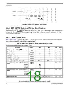
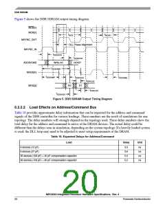
Figure 4 provides the AC test load for the DDR bus.
GVDD/2
Output
Z0 = 50 Ω
RL = 50 Ω
Figure 4. DDR AC Test Load
Table 17. DDR SDRAM Measurement Conditions
Symbol
DDR
Unit
Notes
VTH
MVREF 0.31 V
V
V
1
2
V
0.5 × GVDD
OUT
Notes:
1.Data input threshold measurement point.
2.Data output measurement point.
MPC8540 Integrated Processor Hardware Specifications, Rev. 4
Freescale Semiconductor
19

 FREESCALE [ Freescale ]