DDR SDRAM
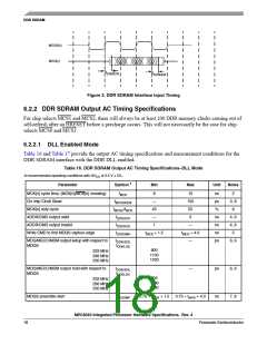
MDQS[n]
MDQ[n]
tDISKEW
tDISKEW
Figure 3. DDR SDRAM Interface Input Timing
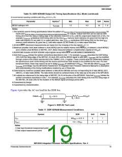
6.2.2 DDR SDRAM Output AC Timing Specifications
For chip selects MCS1 and MCS2, there will always be at least 200 DDR memory clocks coming out of
self-refresh after an HRESET before a precharge occurs. This will not necessarily be the case for chip
selects MCS0 and MCS3.
6.2.2.1 DLL Enabled Mode
Table 16 and Table 17 provide the output AC timing specifications and measurement conditions for the
DDR SDRAM interface with the DDR DLL enabled.
Table 16. DDR SDRAM Output AC Timing Specifications–DLL Mode
At recommended operating conditions with GVDD of 2.5 V 5%.
Parameter
Symbol 1
Min
Max
Unit
Notes
MCK[n] cycle time, (MCK[n]/MCK[n] crossing)
On chip Clock Skew
tMCK
6
10
ns
ps
%
2
tMCKSKEW
tMCKH/tMCK
tDDKHOV
tDDKHOX
tDDSHMH
—
150
3, 8
8
MCK[n] duty cycle
45
55
ADDR/CMD output valid
—
1
3
—
ns
ns
ns
ps
4, 9
4, 9
5
ADDR/CMD output invalid
Write CMD to first MDQS capture edge
tMCK + 1.5
tMCK + 4.0
—
MDQ/MECC/MDM output setup with respect to
MDQS
tDDKHDS,
tDDKLDS
6, 9
900
1100
1200
333 MHz
266 MHz
200 MHz
MDQ/MECC/MDM output hold with respect to
MDQS
tDDKHDX,
tDDKLDX
—
ps
ns
6, 9
7, 8
900
1100
1200
333 MHz
266 MHz
200 MHz
MDQS preamble start
tDDSHMP
0.75 × tMCK + 1.5
0.75 × tMCK + 4.0
MPC8540 Integrated Processor Hardware Specifications, Rev. 4
18
Freescale Semiconductor

 FREESCALE [ Freescale ]