Freescale Semiconductor, Inc.
For a description of the bits contained in the CONFIG register refer to 4.3.2.1 CONFIG
Register.
4.5 Chip Selects
The function of the chip selects is to minimize the amount of external glue logic needed
to interface the MCU to external devices. The MC68HC11F1 has four software config-
ured chip selects that can be enabled in expanded modes. The chip selects for I/O
(CSIO1 and CSIO2) are used for I/O expansion. The program chip select (CSPROG)
is used with an external memory that contains the program code and reset vectors.
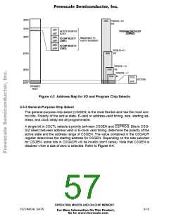
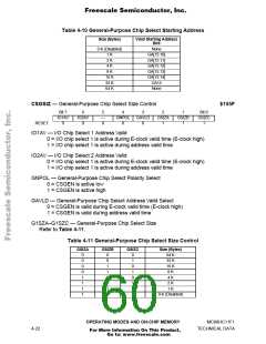
The general-purpose chip select (CSGEN) is the most flexible and is used to enable
external devices.
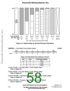
Such factors as polarity, block size, base address and clock stretching can be con-
trolled using the four chip-select control registers. When a port G pin is not used for
chip select functions it can be used for general-purpose I/O.
When enabled, a chip select signal is asserted whenever the CPU makes an access
to a designated range of addresses. Bus control signals and chip select signals are
synchronous with the external E clock signal. For more information refer to Table A–
7. Expansion Bus Timing in APPENDIX A ELECTRICAL CHARACTERISTICS. The
length of the external E clock cycle to which the external device is synchronized can
be stretched to accommodate devices that are slower than the MCU.
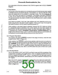
4.5.1 Program Chip Select
The program chip select (CSPROG) is active in the range of memory where the main
program exists. Refer to Figure 4-3.
When enabled, the CSPROG is active during address valid time and is an active-low
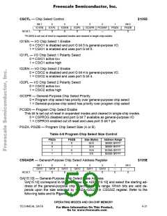
signal. Although the general-purpose chip select has priority over the program chip se-
lect, CSPROG can be raised to a higher priority level by setting the GCSPR bit in
CSCTL register. Bits in CSCTL enable the program chip select and determine its ad-
dress range and priority level. Bits in CSSTRH select from zero to three clock cycles
of delay.
4.5.2 I/O Chip Selects
The I/O chip selects (CSIO1 and CSIO2) are fixed in size and fill the remainder of the
4-Kbyte block occupied by the register block. CSIO1 is mapped at $x060–$x7FF and
CSIO2 is mapped at $x800–$xFFF, where “x” corresponds to the high-order nibble of
the register block base address, represented by the value contained in REG[3:0] in the
INIT register.
Bits in the CSCTL register determine the polarity of the active state and enable both I/
O chip selects. Bits in CSGSIZ select whether each chip select is active for address-
valid or E-valid time. Bits in CSSTRH select from zero to three clock cycles of delay.
Refer to Figure 4-3.
OPERATING MODES AND ON-CHIP MEMORY
MC68HC11F1
4-18
TECHNICAL DATA
For More Information On This Product,
Go to: www.freescale.com

 FREESCALE [ Freescale ]