Analog-to-Digital Converter (ADC)
I/O Registers
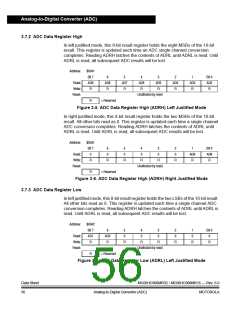
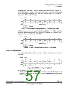
In right justified mode, this 8-bit result register holds the eight LSBs of the 10-bit
result. This register is updated each time an ADC conversion completes. Reading
ADRH latches the contents of ADRL until ADRL is read. Until ADRL is read, all
subsequent ADC results will be lost.
Address:
$0042
Bit 7
AD7
R
6
AD6
R
5
AD5
R
4
AD4
R
3
AD3
R
2
AD2
R
1
AD1
R
Bit 0
AD0
R
Read:
Write:
Reset:
Unaffected by reset
R
= Reserved
Figure 3-8. ADC Data Register Low (ADRL) Right Justified Mode
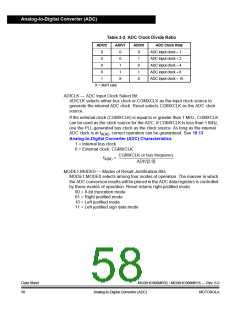
In 8-bit mode, this 8-bit result register holds the eight MSBs of the 10-bit result. This
register is updated each time an ADC conversion completes. In 8-bit mode, this
register contains no interlocking with ADRH.
Address:
$0042
Bit 7
AD9
R
6
AD8
R
5
AD7
R
4
AD6
R
3
AD5
R
2
AD4
R
1
AD3
R
Bit 0
AD2
R
Read:
Write:
Reset:
Unaffected by reset
R
= Reserved
Figure 3-9. ADC Data Register Low (ADRL) 8-Bit Mode
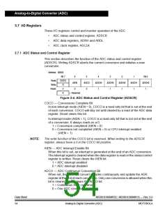
3.7.4 ADC Clock Register
This register selects the clock frequency for the ADC, selecting between modes of
operation.
Address:
$0043
Bit 7
6
5
ADIV0
0
4
ADICLK
0
3
MODE1
0
2
MODE0
1
1
0
0
Bit 0
0
Read:
Write:
Reset:
ADIV2
ADIV1
R
0
0
0
R
= Reserved
Figure 3-10. ADC Clock Register (ADCLK)
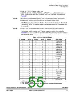
ADIV2:ADIV0 — ADC Clock Prescaler Bits
ADIV2, ADIV1, and ADIV0 form a 3-bit field which selects the divide ratio used
by the ADC to generate the internal ADC clock. Table 3-2 shows the available
clock configurations.
MC68HC908MR32 • MC68HC908MR16 — Rev. 6.0
MOTOROLA Analog-to-Digital Converter (ADC)
Data Sheet
57

 FREESCALE [ Freescale ]