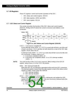
Analog-to-Digital Converter (ADC)
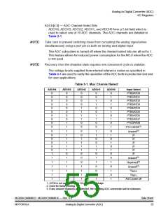
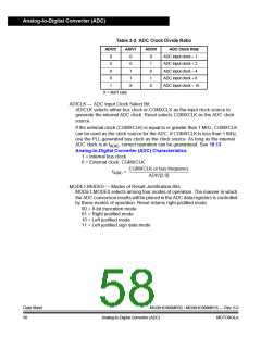
Table 3-2. ADC Clock Divide Ratio
ADIV2
ADIV1
ADIV0
ADC Clock Rate
ADC input clock ÷ 1
ADC input clock ÷ 2
ADC input clock ÷ 4
ADC input clock ÷ 8
ADC input clock ÷ 16
0
0
0
0
1
0
0
1
1
X
0
1
0
1
X
X = don’t care
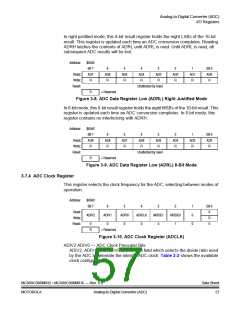
ADICLK — ADC Input Clock Select Bit
ADICLK selects either bus clock or CGMXCLK as the input clock source to
generate the internal ADC clock. Reset selects CGMXCLK as the ADC clock
source.
If the external clock (CGMXCLK) is equal to or greater than 1 MHz, CGMXCLK
can be used as the clock source for the ADC. If CGMXCLK is less than 1 MHz,
use the PLL-generated bus clock as the clock source. As long as the internal
ADC clock is at fADIC, correct operation can be guaranteed. See 19.13
Analog-to-Digital Converter (ADC) Characteristics.
1 = Internal bus clock
0 = External clock, CGMXCLK
CGMXCLK or bus frequency
fADIC
=
ADIV[2:0]
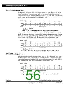
MODE1:MODE0 — Modes of Result Justification Bits
MODE1:MODE0 selects among four modes of operation. The manner in which
the ADC conversion results will be placed in the ADC data registers is controlled
by these modes of operation. Reset returns right-justified mode.
00 = 8-bit truncation mode
01 = Right justified mode
10 = Left justified mode
11 = Left justified sign data mode
Data Sheet
58
MC68HC908MR32 • MC68HC908MR16 — Rev. 6.0
Analog-to-Digital Converter (ADC)
MOTOROLA

 FREESCALE [ Freescale ]