Analog-to-Digital Converter (ADC)
I/O Registers
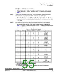
ADCH[4:0] — ADC Channel Select Bits
ADCH4, ADCH3, ADCH2, ADCH1, and ADCH0 form a 5-bit field which is
used to select one of 10 ADC channels. The ADC channels are detailed in
Table 3-1.
NOTE:
NOTE:
Take care to prevent switching noise from corrupting the analog signal when
simultaneously using a port pin as both an analog and digital input.
The ADC subsystem is turned off when the channel select bits are all set to 1.
This feature allows for reduced power consumption for the MCU when the ADC
is not used.
Recovery from the disabled state requires one conversion cycle to stabilize.
The voltage levels supplied from internal reference nodes as specified in
Table 3-1 are used to verify the operation of the ADC both in production test and
for user applications.
Table 3-1. Mux Channel Select
ADCH4
ADCH3
ADCH2
ADCH1
ADCH0
Input Select
PTB0/ATD0
PTB1/ATD1
PTB2/ATD2
PTB3/ATD3
PTB4/ATD4
PTB5/ATD5
PTB6/ATD6
PTB7/ATD7
PTC0/ATD8
0
0
0
0
0
0
0
0
0
0
0
0
0
0
0
0
0
0
1
1
0
0
0
0
1
1
1
1
0
0
0
0
1
1
0
0
1
1
0
0
0
1
0
1
0
1
0
1
0
1
PTC1/ATD9(1)
Unused(2)
0
0
0
0
0
0
1
1
1
1
1
1
1
1
0
1
0
0
1
1
1
1
0
0
1
1
0
0
1
1
0
1
0
1
0
1
0
1
0
0
Ø
Ø
Ø
Ø
Ø
Ø
Unused(2)
Reserved(3)
1
1
0
1
1
Unused(2)
VREFH
1
1
1
1
1
1
1
1
1
1
1
1
0
0
1
1
0
1
0
1
VREFL
ADC power off
1. ATD9 is not available in the 56-pin SDIP package.
2. Used for factory testing.
3. If any unused channels are selected, the resulting ADC conversion will be unknown.
MC68HC908MR32 • MC68HC908MR16 — Rev. 6.0
MOTOROLA Analog-to-Digital Converter (ADC)
Data Sheet
55

 FREESCALE [ Freescale ]