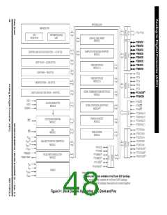
Analog-to-Digital Converter (ADC)
Functional Description
INTERNAL
DATA BUS
PTB/Cx
ADC CHANNEL x
READ PTB/PTC
DISABLE
ADC DATA REGISTERS
CONVERSION
COMPLETE
ADC VOLTAGE IN
ADVIN
INTERRUPT
LOGIC
CHANNEL
ADCH[4:0]
SELECT
ADC
AIEN
COCO
ADC CLOCK
CGMXCLK
CLOCK
GENERATOR
BUS CLOCK
ADIV[2:0]
ADICLK
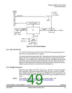
Figure 3-2. ADC Block Diagram
3.3.1 ADC Port I/O Pins
PTC1/ATD9:PTC0/ATD8 and PTB7/ATD7:PTB0/ATD0 are general-purpose I/O
pins that are shared with the ADC channels.
The channel select bits define which ADC channel/port pin will be used as the input
signal. The ADC overrides the port logic when that port is selected by the ADC
multiplexer. The remaining ADC channels/port pins are controlled by the port logic
and can be used as general-purpose input/output (I/O) pins. Writes to the port
register or DDR will not have any effect on the port pin that is selected by the ADC.
Read of a port pin which is in use by the ADC will return a 0.
3.3.2 Voltage Conversion
When the input voltage to the ADC equals VREFH, the ADC converts the signal to
$3FF (full scale). If the input voltage equals VREFL, the ADC converts it to $000.
Input voltages between VREFH and VREFL are straight-line linear conversions. All
other input voltages will result in $3FF if greater than VREFH and $000 if less than
VREFL
.
NOTE:
Input voltage should not exceed the analog supply voltages. See
19.13 Analog-to-Digital Converter (ADC) Characteristics.
MC68HC908MR32 • MC68HC908MR16 — Rev. 6.0
MOTOROLA Analog-to-Digital Converter (ADC)
Data Sheet
49

 FREESCALE [ Freescale ]