Timer Interface A (TIMA)
Functional Description
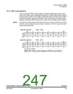
3. In the TIMA channel x registers (TACHxH–TACHxL), write the value for the
required pulse width.
4. In TIMA channel x status and control register (TSCx):
a. Write 0:1 (for unbuffered output compare or PWM signals) or 1:0 (for
buffered output compare or PWM signals) to the mode select bits,
MSxB–MSxA. (See Table 16-2.)
b. Write 1 to the toggle-on-overflow bit, TOVx.
c. Write 1:0 (polarity 1 — to clear output on compare) or 1:1 (polarity 0 —
to set output on compare) to the edge/level select bits, ELSxB–ELSxA.
The output action on compare must force the output to the complement
of the pulse width level. (See Table 16-2.)
NOTE:
In PWM signal generation, do not program the PWM channel to toggle on output
compare. Toggling on output compare prevents reliable 0 percent duty cycle
generation and removes the ability of the channel to self-correct in the event of
software error or noise. Toggling on output compare can also cause incorrect PWM
signal generation when changing the PWM pulse width to a new, much larger
value.
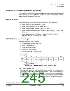
5. In the TIMA status control register (TASC), clear the TIMA stop bit, TSTOP.
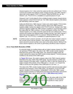
Setting MS0B links channels 0 and 1 and configures them for buffered PWM
operation. The TIMA channel 0 registers (TACH0H–TACH0L) initially control the
buffered PWM output. TIMA status control register 0 (TASC0) controls and
monitors the PWM signal from the linked channels. MS0B takes priority over
MS0A.
Setting MS2B links channels 2 and 3 and configures them for buffered PWM
operation. The TIMA channel 2 registers (TACH2H–TACH2L) initially control the
buffered PWM output. TIMA status control register 2 (TASC2) controls and
monitors the PWM signal from the linked channels. MS2B takes priority over
MS2A.
Clearing the toggle-on-overflow bit, TOVx, inhibits output toggles on TIMA
overflows. Subsequent output compares try to force the output to a state it is
already in and have no effect. The result is a 0 percent duty cycle output.
Setting the channel x maximum duty cycle bit (CHxMAX) and setting the TOVx bit
generates a 100 percent duty cycle output. (See 16.7.4 TIMA Channel Status and
Control Registers.)
MC68HC908MR32 • MC68HC908MR16 — Rev. 6.0
MOTOROLA
Data Sheet
243
Timer Interface A (TIMA)

 FREESCALE [ Freescale ]