Timer Interface A (TIMA)
channel registers (0 or 1) that control the output are the ones written to last. TASC0
controls and monitors the buffered output compare function, and TIMA channel 1
status and control register (TASC1) is unused. While the MS0B bit is set, the
channel 1 pin, PTE5/TCH1A, is available as a general-purpose I/O pin.
Channels 2 and 3 can be linked to form a buffered output compare channel whose
output appears on the PTE6/TCH2A pin. The TIMA channel registers of the linked
pair alternately control the output.
Setting the MS2B bit in TIMA channel 2 status and control register (TASC2) links
channel 2 and channel 3. The output compare value in the TIMA channel 2
registers initially controls the output on the PTE6/TCH2A pin. Writing to the TIMA
channel 3 registers enables the TIMA channel 3 registers to synchronously control
the output after the TIMA overflows. At each subsequent overflow, the TIMA
channel registers (2 or 3) that control the output are the ones written to last. TASC2
controls and monitors the buffered output compare function, and TIMA channel 3
status and control register (TASC3) is unused. While the MS2B bit is set, the
channel 3 pin, PTE7/TCH3A, is available as a general-purpose I/O pin.
NOTE:
In buffered output compare operation, do not write new output compare values to
the currently active channel registers. User software should track the currently
active channel to prevent writing a new value to the active channel. Writing to the
active channel registers is the same as generating unbuffered output compares.
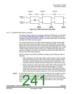
16.3.4 Pulse-Width Modulation (PWM)
By using the toggle-on-overflow feature with an output compare channel, the TIMA
can generate a PWM signal. The value in the TIMA counter modulo registers
determines the period of the PWM signal. The channel pin toggles when the
counter reaches the value in the TIMA counter modulo registers. The time between
overflows is the period of the PWM signal.
As Figure 16-4 shows, the output compare value in the TIMA channel registers
determines the pulse width of the PWM signal. The time between overflow and
output compare is the pulse width. Program the TIMA to clear the channel pin on
output compare if the polarity of the PWM pulse is 1 (ELSxA = 0). Program the
TIMA to set the pin if the polarity of the PWM pulse is 0 (ELSxA = 1).
The value in the TIMA counter modulo registers and the selected prescaler output
determines the frequency of the PWM output. The frequency of an 8-bit PWM
signal is variable in 256 increments. Writing $00FF (255) to the TIMA counter
modulo registers produces a PWM period of 256 times the internal bus clock period
if the prescaler select value is $000 (see 16.7.1 TIMA Status and Control
Register).
The value in the TIMA channel registers determines the pulse width of the PWM
output. The pulse width of an 8-bit PWM signal is variable in 256 increments.
Writing $0080 (128) to the TIMA channel registers produces a duty cycle of
128/256 or 50 percent.
Data Sheet
240
MC68HC908MR32 • MC68HC908MR16 — Rev. 6.0
Timer Interface A (TIMA)
MOTOROLA

 FREESCALE [ Freescale ]