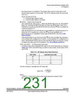
Serial Peripheral Interface Module (SPI)
I/O Registers
(See 15.6.2 Mode Fault Error.) For the state of the SS pin to set the MODF flag,
the MODFEN bit in the SPSCK register must be set. If the MODFEN bit is low for
an SPI master, the SS pin can be used as a general-purpose I/O under the control
of the data direction register of the shared I/O port. With MODFEN high, it is an
input-only pin to the SPI regardless of the state of the data direction register of the
shared I/O port.
The CPU can always read the state of the SS pin by configuring the appropriate
pin as an input and reading the port data register. See Table 15-3.
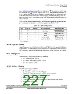
Table 15-3. SPI Configuration
SPE
SPMSTR
MODFEN
SPI Configuration
Not enabled
Slave
State of SS Logic
General-purpose I/O;
SS ignored by SPI
X(1)
0
0
1
1
1
X
X
0
Input-only to SPI
Master
without MODF
General-purpose I/O;
SS ignored by SPI
1
1
1
Master with MODF
Input-only to SPI
1. X = don’t care
15.11.5 VSS (Clock Ground)
SS is the ground return for the serial clock pin, SPSCK, and the ground for the port
V
output buffers. To reduce the ground return path loop and minimize radio frequency
(RF) emissions, connect the ground pin of the slave to the VSS pin of the master.
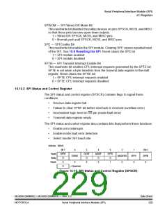
15.12 I/O Registers
Three registers control and monitor SPI operation:
•
•
•
SPI control register, SPCR
SPI status and control register, SPSCR
SPI data register, SPDR
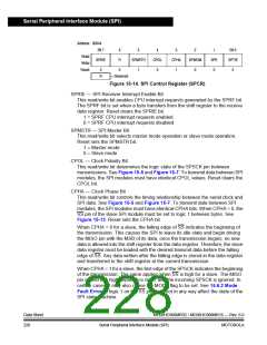
15.12.1 SPI Control Register
The SPI control register (SPCR):
•
•
•
•
•
•
Enables SPI module interrupt requests
Selects CPU interrupt requests or DMA service requests
Configures the SPI module as master or slave
Selects serial clock polarity and phase
Configures the SPSCK, MOSI, and MISO pins as open-drain outputs
Enables the SPI module
MC68HC908MR32 • MC68HC908MR16 — Rev. 6.0
MOTOROLA Serial Peripheral Interface Module (SPI)
Data Sheet
227

 FREESCALE [ Freescale ]