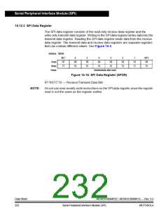
Serial Peripheral Interface Module (SPI)
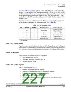
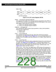
Address: $0044
Bit 7
6
5
SPMSTR
1
4
CPOL
0
3
CPHA
1
2
SPWOM
0
1
SPE
0
Bit 0
SPTIE
0
Read:
Write:
Reset:
SPRIE
R
0
0
R
= Reserved
Figure 15-14. SPI Control Register (SPCR)
SPRIE — SPI Receiver Interrupt Enable Bit
This read/write bit enables CPU interrupt requests generated by the SPRF bit.
The SPRF bit is set when a byte transfers from the shift register to the receive
data register. Reset clears the SPRIE bit.
1 = SPRF CPU interrupt requests enabled
0 = SPRF CPU interrupt requests disabled
SPMSTR — SPI Master Bit
This read/write bit selects master mode operation or slave mode operation.
Reset sets the SPMSTR bit.
1 = Master mode
0 = Slave mode
CPOL — Clock Polarity Bit
This read/write bit determines the logic state of the SPSCK pin between
transmissions. See Figure 15-5 and Figure 15-7. To transmit data between SPI
modules, the SPI modules must have identical CPOL values. Reset clears the
CPOL bit.
CPHA — Clock Phase Bit
This read/write bit controls the timing relationship between the serial clock and
SPI data. See Figure 15-5 and Figure 15-7. To transmit data between SPI
modules, the SPI modules must have identical CPHA bits. When CPHA = 0, the
SS pin of the slave SPI module must be set to logic 1 between bytes. See
Figure 15-13. Reset sets the CPHA bit.
When CPHA = 0 for a slave, the falling edge of SS indicates the beginning of
the transmission. This causes the SPI to leave its idle state and begin driving
the MISO pin with the MSB of its data, once the transmission begins, no new
data is allowed into the shift register from the data register. Therefore, the slave
data register must be loaded with the desired transmit data before the falling
edge of SS. Any data written after the falling edge is stored in the data register
and transferred to the shift register at the current transmission.
When CPHA = 1 for a slave, the first edge of the SPSCK indicates the beginning
of the transmission. The same applies when SS is high for a slave. The MISO
pin is held in a high-impedance state, and the incoming SPSCK is ignored. In
certain cases, it may also cause the MODF flag to be set. See 15.6.2 Mode
Fault Error. A logic 1 on the SS pin does not in any way affect the state of the
SPI state machine.
Data Sheet
228
MC68HC908MR32 • MC68HC908MR16 — Rev. 6.0
Serial Peripheral Interface Module (SPI)
MOTOROLA

 FREESCALE [ Freescale ]