Serial Peripheral Interface Module (SPI)
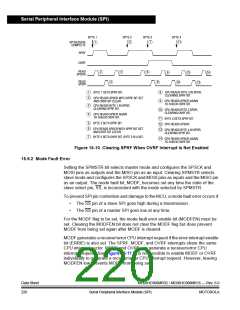
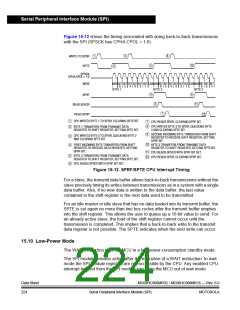
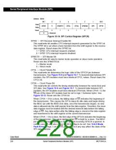
Figure 15-12 shows the timing associated with doing back-to-back transmissions
with the SPI (SPSCK has CPHA:CPOL = 1:0).
1
3
8
WRITE TO SPDR
SPTE
5
10
2
SPSCK
CPHA:CPOL = 1:0
MOSI
MSBBIT BIT BIT BIT BIT BIT LSBMSBBIT BIT BIT BIT BIT BIT LSBMSBBIT BIT BIT
3
6
BYTE 1
5
4
3
2
1
6
BYTE 2
5
4
2
1
6
BYTE 3
5
4
4
9
SPRF
READ SPSCR
READ SPDR
6
11
7
12
1
2
CPU WRITES BYTE 1 TO SPDR, CLEARING SPTE BIT.
7
8
CPU READS SPDR, CLEARING SPRF BIT.
CPU WRITES BYTE 3 TO SPDR, QUEUEING BYTE
3 AND CLEARING SPTE BIT.
BYTE 1 TRANSFERS FROM TRANSMIT DATA
REGISTER TO SHIFT REGISTER, SETTING SPTE BIT.
9
SECOND INCOMING BYTE TRANSFERS FROM SHIFT
REGISTER TO RECEIVE DATA REGISTER, SETTING
SPRF BIT.
CPU WRITES BYTE 2 TO SPDR, QUEUEING BYTE 2
AND CLEARING SPTE BIT.
3
4
10
FIRST INCOMING BYTE TRANSFERS FROM SHIFT
REGISTER TO RECEIVE DATA REGISTER, SETTING
SPRF BIT.
BYTE 3 TRANSFERS FROM TRANSMIT DATA
REGISTER TO SHIFT REGISTER, SETTING SPTE BIT.
11
12
CPU READS SPSCR WITH SPRF BIT SET.
CPU READS SPDR, CLEARING SPRF BIT.
5
6
BYTE 2 TRANSFERS FROM TRANSMIT DATA
REGISTER TO SHIFT REGISTER, SETTING SPTE BIT.
CPU READS SPSCR WITH SPRF BIT SET.
Figure 15-12. SPRF/SPTE CPU Interrupt Timing
For a slave, the transmit data buffer allows back-to-back transmissions without the
slave precisely timing its writes between transmissions as in a system with a single
data buffer. Also, if no new data is written to the data buffer, the last value
contained in the shift register is the next data word to be transmitted.
For an idle master or idle slave that has no data loaded into its transmit buffer, the
SPTE is set again no more than two bus cycles after the transmit buffer empties
into the shift register. This allows the user to queue up a 16-bit value to send. For
an already active slave, the load of the shift register cannot occur until the
transmission is completed. This implies that a back-to-back write to the transmit
data register is not possible. The SPTE indicates when the next write can occur.
15.10 Low-Power Mode
The WAIT instruction puts the MCU in a low power-consumption standby mode.
The SPI module remains active after the execution of a WAIT instruction. In wait
mode the SPI module registers are not accessible by the CPU. Any enabled CPU
interrupt request from the SPI module can bring the MCU out of wait mode.
Data Sheet
224
MC68HC908MR32 • MC68HC908MR16 — Rev. 6.0
Serial Peripheral Interface Module (SPI)
MOTOROLA

 FREESCALE [ Freescale ]