Pulse-Width Modulator for Motor Control (PWMMC)
FINT1 — Fault 1 Interrupt Enable Bit
This read/write bit allows the CPU interrupt caused by faults on fault pin 1 to be
enabled. The fault protection circuitry is independent of this bit and will always
be active. If a fault is detected, the PWM pins will still be disabled according to
the disable mapping register.
1 = Fault pin 1 will cause CPU interrupts.
0 = Fault pin 1 will not cause CPU interrupts.
FMODE1 —Fault Mode Selection for Fault Pin 1 Bit
(automatic versus manual mode)
This read/write bit allows the user to select between automatic and manual
mode faults. For further descriptions of each mode, see 12.6 Fault Protection.
1 = Automatic mode
0 = Manual mode
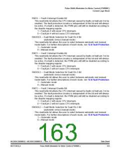
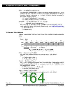
12.9.9 Fault Status Register
The fault status register (FSR) is a read-only register that indicates the current fault
status.
Address:
$0023
Bit 7
6
5
4
3
2
1
Bit 0
Read:
Write:
Reset:
FPIN4
FFLAG4
FPIN3
FFLAG3
FPIN2
FFLAG2
FPIN1
FFLAG1
U
0
U
0
U
0
U
0
= Unimplemented
U = Unaffected
Figure 12-44. Fault Status Register (FSR)
FPIN4 — State of Fault Pin 4 Bit
This read-only bit allows the user to read the current state of fault
pin 4.
1 = Fault pin 4 is at logic 1.
0 = Fault pin 4 is at logic 0.
FFLAG4 — Fault Event Flag 4
The FFLAG4 event bit is set within two CPU cycles after a rising edge on fault
pin 4. To clear the FFLAG4 bit, the user must write a 1 to the FTACK4 bit in the
fault acknowledge register.
1 = A fault has occurred on fault pin 4.
0 = No new fault on fault pin 4
FPIN3 — State of Fault Pin 3 Bit
This read-only bit allows the user to read the current state of fault
pin 3.
1 = Fault pin 3 is at logic 1.
0 = Fault pin 3 is at logic 0.
Data Sheet
164
MC68HC908MR32 • MC68HC908MR16 — Rev. 6.0
Pulse-Width Modulator for Motor Control (PWMMC)
MOTOROLA

 FREESCALE [ Freescale ]