Pulse-Width Modulator for Motor Control (PWMMC)
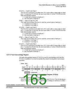
FTACK3 — Fault Acknowledge 3 Bit
The FTACK3 bit is used to acknowledge and clear FFLAG3. This bit will always
read 0. Writing a 1 to this bit will clear FFLAG3. Writing a 0 will have no effect.
FTACK2 — Fault Acknowledge 2 Bit
The FTACK2 bit is used to acknowledge and clear FFLAG2. This bit will always
read 0. Writing a 1 to this bit will clear FFLAG2. Writing a 0 will have no effect.
FTACK1 — Fault Acknowledge 1 Bit
The FTACK1 bit is used to acknowledge and clear FFLAG1. This bit will always
read 0. Writing a 1 to this bit will clear FFLAG1. Writing a 0 will have no effect.
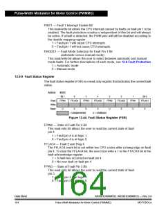
DT6 — Dead-Time 6 Bit
Current sensing pin IS3 is monitored immediately before dead-time ends due to
the assertion of PWM6.
DT5 — Dead-Time 5 Bit
Current sensing pin IS3 is monitored immediately before dead-time ends due to
the assertion of PWM5.
DT4 — Dead-Time 4 Bit
Current sensing pin IS2 is monitored immediately before dead-time ends due to
the assertion of PWM4.
DT3 — Dead-Time 3 Bit
Current sensing pin IS2 is monitored immediately before dead-time ends due to
the assertion of PWM3.
DT2 — Dead-Time 2 Bit
Current sensing pin IS1 is monitored immediately before dead-time ends due to
the assertion of PWM2.
DT1 — Dead-Time 1 Bit
Current sensing pin IS1 is monitored immediately before dead-time ends due to
the assertion of PWM1.
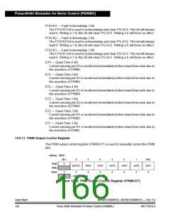
12.9.11 PWM Output Control Register
The PWM output control register (PWMOUT) is used to manually control the PWM
pins.
Address: $0025
Bit 7
0
6
OUTCTL
0
5
OUT6
0
4
OUT5
0
3
OUT4
0
2
OUT3
0
1
OUT2
0
Bit 0
OUT1
0
Read:
Write:
Reset:
0
= Unimplemented
Figure 12-46. PWM Output Control Register (PWMOUT)
Data Sheet
166
MC68HC908MR32 • MC68HC908MR16 — Rev. 6.0
Pulse-Width Modulator for Motor Control (PWMMC) MOTOROLA

 FREESCALE [ Freescale ]