Pulse-Width Modulator for Motor Control (PWMMC)
Control Logic Block
FFLAG3 — Fault Event Flag 3
The FFLAG3 event bit is set within two CPU cycles after a rising edge on fault
pin 3. To clear the FFLAG3 bit, the user must write a 1 to the FTACK3 bit in the
fault acknowledge register.
1 = A fault has occurred on fault pin 3.
0 = No new fault on fault pin 3.
FPIN2 — State of Fault Pin 2 Bit
This read-only bit allows the user to read the current state of fault pin 2.
1 = Fault pin 2 is at logic 1.
0 = Fault pin 2 is at logic 0.
FFLAG2 — Fault Event Flag 2
The FFLAG2 event bit is set within two CPU cycles after a rising edge on fault
pin 2. To clear the FFLAG2 bit, the user must write a 1 to the FTACK2 bit in the
fault acknowledge register.
1 = A fault has occurred on fault pin 2.
0 = No new fault on fault pin 2
FPIN1 — State of Fault Pin 1 Bit
This read-only bit allows the user to read the current state of fault pin 1.
1 = Fault pin 1 is at logic 1.
0 = Fault pin 1 is at logic 0.
FFLAG1 — Fault Event Flag 1
The FFLAG1 event bit is set within two CPU cycles after a rising edge on fault
pin 1. To clear the FFLAG1 bit, the user must write a 1 to the FTACK1 bit in the
fault acknowledge register.
1 = A fault has occurred on fault pin 1.
0 = No new fault on fault pin 1.
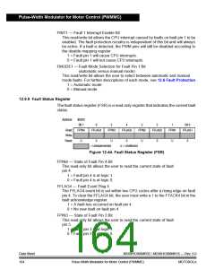
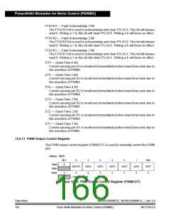
12.9.10 Fault Acknowledge Register
The fault acknowledge register (FTACK) is used to acknowledge and clear the
FFLAGs. In addition, it is used to monitor the current sensing bits to test proper
operation.
Address: $0024
Bit 7
0
6
5
4
DT5
3
2
DT3
1
Bit 0
DT1
Read:
Write:
Reset:
0
FTACK4
0
DT6
DT4
DT2
FTACK3
0
FTACK2
0
FTACK1
0
0
0
0
0
= Unimplemented
Figure 12-45. Fault Acknowledge Register (FTACK)
FTACK4 — Fault Acknowledge 4 Bit
The FTACK4 bit is used to acknowledge and clear FFLAG4. This bit will always
read 0. Writing a 1 to this bit will clear FFLAG4. Writing a 0 will have no effect.
MC68HC908MR32 • MC68HC908MR16 — Rev. 6.0
MOTOROLA Pulse-Width Modulator for Motor Control (PWMMC)
Data Sheet
165

 FREESCALE [ Freescale ]