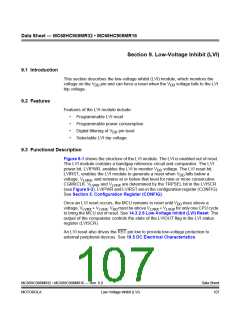
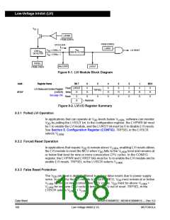
Low-Voltage Inhibit (LVI)
VDD
LVIPWR
FROM CONFIG
FROM CONFIG
LVIRST
CPU CLOCK
VDD
DIGITAL FILTER
VDD > LVItrip = 0
VDD < LVItrip = 1
LVI RESET
LOW VDD
DETECTOR
TRPSEL
ANLGTRIP
LVIOUT
FROM LVISCR
Figure 9-1. LVI Module Block Diagram
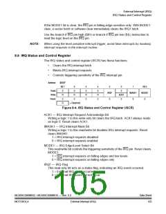
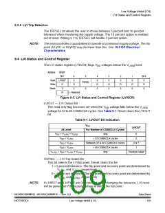
Addr.
Register Name
Bit 7
6
5
TRPSEL
0
4
0
3
0
2
0
1
Bit 0
Read: LVIOUT
0
0
R
0
0
R
0
LVI Status and Control Register
See page 109.
$FE0F
(LVISCR) Write:
R
0
R
R
0
R
0
R
0
Reset:
0
= Reserved
R
Figure 9-2. LVI I/O Register Summary
9.3.1 Polled LVI Operation
In applications that can operate at VDD levels below VLVRX, software can monitor
DD by polling the LVIOUT bit. In the configuration register, the LVIPWR bit must
V
be 1 to enable the LVI module, and the LVIRST bit must be 0 to disable LVI resets.
See Section 5. Configuration Register (CONFIG). TRPSEL in the LVISCR
selects VLVRX
.
9.3.2 Forced Reset Operation
In applications that require VDD to remain above VLVRX, enabling LVI resets allows
the LVI module to reset the MCU when VDD falls to the VLVRX level and remains at
or below that level for nine or more consecutive CPU cycles. In the CONFIG
register, the LVIPWR and LVIRST bits must be 1s to enable the LVI module and to
enable LVI resets. TRPSEL in the LVISCR selects VLVRX
.
9.3.3 False Reset Protection
The VDD pin level is digitally filtered to reduce false resets due to power supply
noise. In order for the LVI module to reset the MCU, VDD must remain at or below
VLVRX for nine or more consecutive CPU cycles. VDD must be above VLVRX
VLVHX for only one CPU cycle to bring the MCU out of reset. TRPSEL in the
+
LVISCR selects VLVRX + VLVHX
.
Data Sheet
108
MC68HC908MR32 • MC68HC908MR16 — Rev. 6.0
MOTOROLA
Low-Voltage Inhibit (LVI)

 FREESCALE [ Freescale ]