Data Sheet — MC68HC908MR32 • MC68HC908MR16
Section 9. Low-Voltage Inhibit (LVI)
9.1 Introduction
9.2 Features
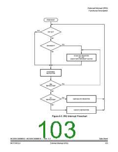
This section describes the low-voltage inhibit (LVI) module, which monitors the
voltage on the VDD pin and can force a reset when the VDD voltage falls to the LVI
trip voltage.
Features of the LVI module include:
•
•
•
•
Programmable LVI reset
Programmable power consumption
Digital filtering of VDD pin level
Selectable LVI trip voltage
9.3 Functional Description
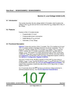
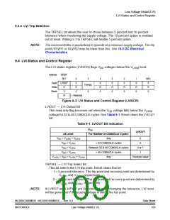
Figure 9-1 shows the structure of the LVI module. The LVI is enabled out of reset.
The LVI module contains a bandgap reference circuit and comparator. The LVI
power bit, LVIPWR, enables the LVI to monitor VDD voltage. The LVI reset bit,
LVIRST, enables the LVI module to generate a reset when VDD falls below a
voltage, VLVRX, and remains at or below that level for nine or more consecutive
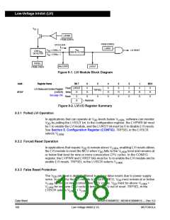
CGMXCLK. VLVRX and VLVHX are determined by the TRPSEL bit in the LVISCR
(see Figure 9-2). LVIPWR and LVIRST are in the configuration register (CONFIG).
See Section 5. Configuration Register (CONFIG).
Once an LVI reset occurs, the MCU remains in reset until VDD rises above a
voltage, VLVRX + VLVHX. VDD must be above VLVRX + VLVHX for only one CPU cycle
to bring the MCU out of reset. See 14.3.2.6 Low-Voltage Inhibit (LVI) Reset. The
output of the comparator controls the state of the LVIOUT flag in the LVI status
register (LVISCR).
An LVI reset also drives the RST pin low to provide low-voltage protection to
external peripheral devices. See 19.5 DC Electrical Characteristics.
MC68HC908MR32 • MC68HC908MR16 — Rev. 6.0
MOTOROLA Low-Voltage Inhibit (LVI)
Data Sheet
107

 FREESCALE [ Freescale ]