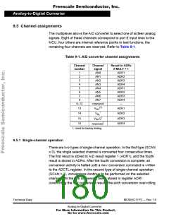
Freescale Semiconductor, Inc.
Analog-to-Digital Converter
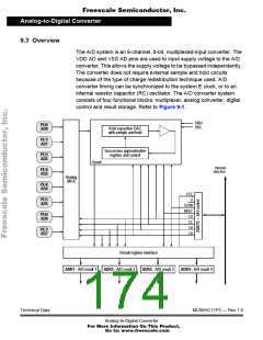
9.3.2 Analog converter
Conversion of an analog input selected by the multiplexer occurs in this
block. It contains a digital-to-analog capacitor (DAC) array, a
comparator, and a successive approximation register (SAR). Each
conversion is a sequence of eight comparison operations, beginning
with the most significant bit (MSB). Each comparison determines the
value of a bit in the SAR.
The DAC array performs two functions. It acts as a sample and hold
circuit during the entire conversion sequence, and provides comparison
voltage to the comparator during each successive comparison.
The result of each successive comparison is stored in the SAR. When a
conversion sequence is complete, the contents of the SAR are
transferred to the appropriate result register.
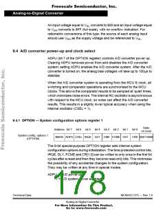
A charge pump provides switching voltage to the gates of analog
switches in the multiplexer. Charge pump output must stabilize between
7 and 8 volts within up to 100 µs before the converter can be used. The
charge pump is enabled by the ADPU bit in the OPTION register.
9.3.3 Digital control
All A/D converter operations are controlled by bits in register ADCTL. In
addition to selecting the analog input to be converted, ADCTL bits
indicate conversion status, and control whether single or continuous
conversions are performed. Finally, the ADCTL bits determine whether
conversions are performed on single or multiple channels.
9.3.4 Result registers
Four 8-bit registers (ADR1 – ADR4) store conversion results. Each of
these registers can be accessed by the processor in the CPU. The
conversion complete flag (CCF) indicates when valid data is present in
the result registers. The result registers are written during a portion of the
system clock cycle when reads do not occur, so there is no conflict.
Technical Data
MC68HC11P2 — Rev 1.0
Analog-to-Digital Converter
For More Information On This Product,
Go to: www.freescale.com

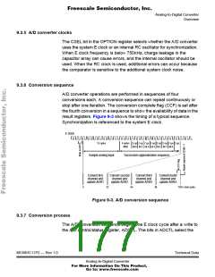
 FREESCALE [ Freescale ]