Freescale Semiconductor, Inc.
Analog-to-Digital Converter
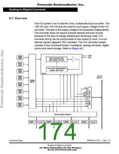
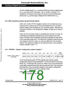
9.3 Overview
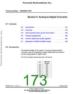
The A/D system is an 8-channel, 8-bit, multiplexed-input converter. The
VDD AD and VSS AD pins are used to input supply voltage to the A/D
converter. This allows the supply voltage to be bypassed independently.
The converter does not require external sample and hold circuits
because of the type of charge redistribution technique used. A/D
converter timing can be synchronized to the system E clock, or to an
internal resistor capacitor (RC) oscillator. The A/D converter system
consists of four functional blocks: multiplexer, analog converter, digital
control and result storage. Refer to Figure 9-1.
VRH
VRL
PE0/
AD0
8-bit capacitive DAC
with sample and hold
PE1/
AD1
Successive approximation
register and control
PE2/
AD2
Result
Internal
data bus
PE3/
AD3
Analog
MUX
PE4/
AD4
CCF
0
PE5/
AD5
SCAN
MULT
CD
PE6/
AD6
CC
CB
PE7/
AD7
CA
Result register interface
ADR1 - A/D result 1
ADR2 - A/D result 2
ADR3 - A/D result 3
ADR4 - A/D result 4
Technical Data
MC68HC11P2 — Rev 1.0
Analog-to-Digital Converter
For More Information On This Product,
Go to: www.freescale.com

 FREESCALE [ Freescale ]