Freescale Semiconductor, Inc.
Technical Data — MC68HC11P2
Section 9. Analog-to-Digital Converter
9.1 Contents
9.2
9.3
9.4
9.5
9.6
9.7
Introduction. . . . . . . . . . . . . . . . . . . . . . . . . . . . . . . . . . . . . .173
Overview . . . . . . . . . . . . . . . . . . . . . . . . . . . . . . . . . . . . . . . .174
A/D converter power-up and clock select . . . . . . . . . . . . .178
Channel assignments. . . . . . . . . . . . . . . . . . . . . . . . . . . . . .180
Control, status and results registers . . . . . . . . . . . . . . . . .181
Operation in STOP and WAIT modes . . . . . . . . . . . . . . . . .184
9.2 Introduction
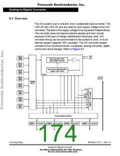
The analog-to-digital (A/D) system, a successive approximation
converter, uses an all-capacitive charge redistribution technique to
convert analog signals to digital values.
The A/D converter shares input pins with port E:
Alternate
Pin
function
PE0
PE1
PE2
PE3
PE4
PE5
PE6
PE7
AD0
AD1
AD2
AD3
AD4
AD5
AD6
AD7
MC68HC11P2 — Rev 1.0
Technical Data
Analog-to-Digital Converter
For More Information On This Product,
Go to: www.freescale.com

 FREESCALE [ Freescale ]