Freescale Semiconductor, Inc.
Analog-to-Digital Converter
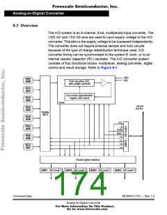
Overview
9.3.1 Multiplexer
The multiplexer selects one of 16 inputs for conversion. Input selection
is controlled by the value of bits CD – CA in the ADCTL register. The
eight port E pins are fixed-direction analog inputs to the multiplexer, and
additional internal analog signal lines are routed to it.
Port E pins can also be used as digital inputs. Digital reads of port E pins
are not recommended during the sample portion of an A/D conversion
cycle, when the gate signal to the N-channel input gate is on. Because
no P-channel devices are directly connected to either input pins or
reference voltage pins, voltages above VDD do not cause a latchup
problem, although current should be limited according to maximum
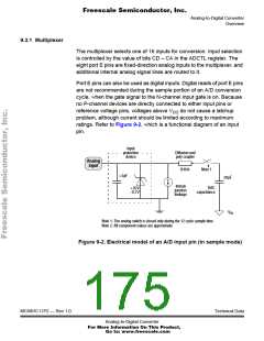
ratings. Refer to Figure 9-2, which is a functional diagram of an input
pin.
Input
protection
device
Diffusion and
poly coupler
Analog
input
ð4k¾
Note 1
<2pF
20pF
400nA
junction
leakage
DAC
capacitance
+20V
–0.7V
V
RL
Note 1: The analog switch is closed only during the 12 cycle sample time
Note 2: All component values are approximate
Figure 9-2. Electrical model of an A/D input pin (in sample mode)
MC68HC11P2 — Rev 1.0
Technical Data
Analog-to-Digital Converter
For More Information On This Product,
Go to: www.freescale.com

 FREESCALE [ Freescale ]