Freescale Semiconductor, Inc.
Timing System
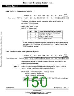
8.5.6 TCTL1 — Timer control register 1
State
on reset
Address bit 7 bit 6 bit 5 bit 4 bit 3 bit 2 bit 1 bit 0
Timer control 1 (TCTL1)
$0020 OM2 OL2 OM3 OL3 OM4 OL4 OM5 OL5 0000 0000
The bits of this register specify the action taken as a result of a
successful OCx compare.
OM[2:5] — Output mode
OL[2:5] — Output level
OMx
OLx
Action taken on successful compare
Timer disconnected from OCx pin logic
Toggle OCx output line
0
0
1
1
0
1
0
1
Clear OCx output line to 0
Set OCx output line to 1
These control bit pairs are encoded to specify the action taken after a
successful OCx compare. OC5 functions only if the I4/O5 bit in the
PACTL register is clear.
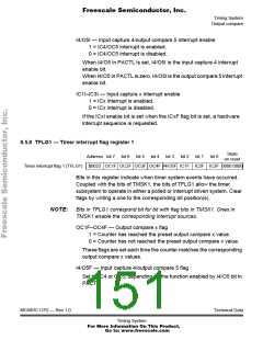
8.5.7 TMSK1 — Timer interrupt mask register 1
State
on reset
Address bit 7 bit 6 bit 5 bit 4 bit 3 bit 2 bit 1 bit 0
Timer interrupt mask 1 (TMSK1) $0022 OC1I OC2I OC3I OC4I I4/O5I IC1I
IC2I
IC3I 0000 0000
Use this 8-bit register to enable or inhibit the timer input capture and
output compare interrupts.
NOTE: Bits in TMSK1 correspond bit for bit with flag bits in TFLG1. Ones in
TMSK1 enable the corresponding interrupt sources.
OC1I–OC4I — Output compare x interrupt enable
1 = OCx interrupt is enabled.
0 = OCx interrupt is disabled.
If the OCxI enable bit is set when the OCxF flag bit is set, a hardware
interrupt sequence is requested.
Technical Data
MC68HC11P2 — Rev 1.0
Timing System
For More Information On This Product,
Go to: www.freescale.com

 FREESCALE [ Freescale ]