Freescale Semiconductor, Inc.
Timing System
Output compare
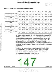
8.5.1 TOC1–TOC4 — Timer output compare registers
State
on reset
Address bit 7 bit 6 bit 5 bit 4 bit 3 bit 2 bit 1 bit 0
Timer output compare 1 (TOC1)
high
$0016 (bit 15) (14)
$0017 (bit 7) (6)
$0018 (bit 15) (14)
$0019 (bit 7) (6)
$001A (bit 15) (14)
$001B (bit 7) (6)
$001C (bit 15) (14)
$001D (bit 7) (6)
(13)
(5)
(12)
(4)
(11)
(3)
(10)
(2)
(9) (bit 8) 1111 1111
(1) (bit 0) 1111 1111
(9) (bit 8) 1111 1111
(1) (bit 0) 1111 1111
(9) (bit 8) 1111 1111
(1) (bit 0) 1111 1111
(9) (bit 8) 1111 1111
(1) (bit 0) 1111 1111
Timer output compare 1 (TOC1)
low
Timer output compare 2 (TOC2)
high
(13)
(5)
(12)
(4)
(11)
(3)
(10)
(2)
Timer output compare 2 (TOC2)
low
Timer output compare 3 (TOC3)
high
(13)
(5)
(12)
(4)
(11)
(3)
(10)
(2)
Timer output compare 3 (TOC3)
low
Timer output compare 4 (TOC4)
high
(13)
(5)
(12)
(4)
(11)
(3)
(10)
(2)
Timer output compare 4 (TOC4)
low
All output compare registers are 16-bit read-write. Each is initialized to
$FFFF at reset. If an output compare register is not used for an output
compare function, it can be used as a storage location. A write to the
high-order byte of an output compare register pair inhibits the output
compare function for one bus cycle. This inhibition prevents
inappropriate subsequent comparisons. Coherency requires a complete
16-bit read or write. However, if coherency is not needed, byte accesses
can be used.
For output compare functions, write a comparison value to output
compare registers TOC1–TOC4 and TI4/O5. When TCNT value
matches the comparison value, specified pin actions occur.
All TOCx register pairs reset to ones ($FFFF).
MC68HC11P2 — Rev 1.0
Technical Data
Timing System
For More Information On This Product,
Go to: www.freescale.com

 FREESCALE [ Freescale ]