Freescale Semiconductor, Inc.
Timing System
Output compare
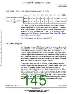
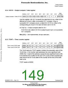
8.5.4 OC1D — Output compare 1 data register
State
on reset
Address bit 7 bit 6 bit 5 bit 4 bit 3 bit 2 bit 1 bit 0
Output compare 1 data (OC1D) $000D OC1D7OC1D6OC1D5OC1D4OC1D3
0
0
0
0000 0000
Use this register with OC1 to specify the data that is to be written to the
affected pin of port A after a successful OC1 compare. When a
successful OC1 compare occurs, a data bit in OC1D is written to the
corresponding pin of port A for each bit that is set in OC1M.
OC1D[7:3] — Output compare data for OC1
If OC1Mx is set, data in OC1Dx is output to port A pin x on successful
OC1 compares.
Bits [2:0] — Not implemented; always read zero
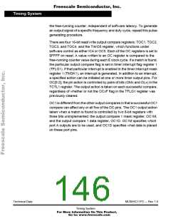
8.5.5 TCNT — Timer counter register
State
on reset
Address bit 7 bit 6 bit 5 bit 4 bit 3 bit 2 bit 1 bit 0
Timer count (TCNT) high
Timer count (TCNT) low
$000E (bit 15) (14)
$000F (bit 7) (6)
(13)
(5)
(12)
(4)
(11)
(3)
(10)
(2)
(9) (bit 8) 0000 0000
(1) (bit 0) 0000 0000
The 16-bit read-only TCNT register contains the prescaled value of the
16-bit timer. A full counter read addresses the more significant byte
(MSB) first. A read of this address causes the less significant byte (LSB)
to be latched into a buffer for the next CPU cycle so that a double-byte
read returns the full 16-bit state of the counter at the time of the MSB
read cycle.
TCNT resets to $0000.
MC68HC11P2 — Rev 1.0
Technical Data
Timing System
For More Information On This Product,
Go to: www.freescale.com

 FREESCALE [ Freescale ]