Freescale Semiconductor, Inc.
Timing System
the free-running counter, independent of software latency. To generate
an output signal of a specific frequency and duty cycle, repeat this pulse-
generating procedure.
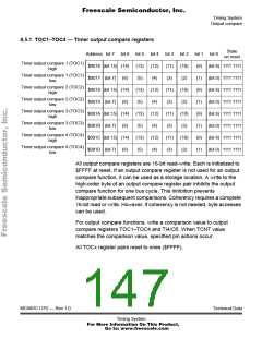
There are four 16-bit read/write output compare registers: TOC1, TOC2,
TOC3, and TOC4, and the TI4/O5 register, which functions under
software control as either IC4 or OC5. Each of the OC registers is set to
$FFFF on reset. A value written to an OC register is compared to the
free-running counter value during each E clock cycle. If a match is found,
the particular output compare flag is set in timer interrupt flag register 1
(TFLG1). If that particular interrupt is enabled in the timer interrupt mask
register 1 (TMSK1), an interrupt is generated. In addition to an interrupt,
a specified action can be initiated at one or more timer output pins. For
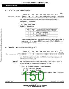
OC[5:2], the pin action is controlled by pairs of bits (OMx and OLx) in the
TCTL1 register. The output action is taken on each successful compare,
regardless of whether or not the OCxF flag in the TFLG1 register was
previously cleared.
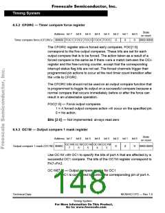
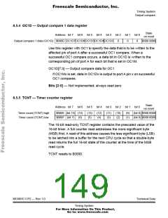
OC1 is different from the other output compares in that a successful OC1
compare can affect any or all five of the OC pins. The OC1 output action
taken when a match is found is controlled by two 8-bit registers with
three bits unimplemented: the output compare 1 mask register, OC1M,
and the output compare 1 data register, OC1D. OC1M specifies which
port A outputs are to be used, and OC1D specifies what data is placed
on these port pins.
Technical Data
MC68HC11P2 — Rev 1.0
Timing System
For More Information On This Product,
Go to: www.freescale.com

 FREESCALE [ Freescale ]