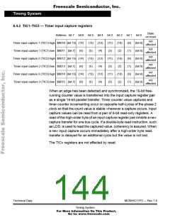
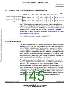
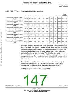
Freescale Semiconductor, Inc.
Timing System
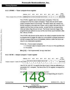
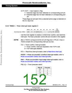
8.5.2 CFORC — Timer compare force register
State
on reset
Address bit 7 bit 6 bit 5 bit 4 bit 3 bit 2 bit 1 bit 0
Timer compare force (CFORC) $000B FOC1 FOC2 FOC3 FOC4 FOC5
0
0
0
0000 0000
The CFORC register allows forced early compares. FOC[1:5]
correspond to the five output compares. These bits are set for each
output compare that is to be forced. The action taken as a result of a
forced compare is the same as if there were a match between the OCx
register and the free-running counter, except that the corresponding
interrupt status flag bits are not set. The forced channels trigger their
programmed pin actions to occur at the next timer count transition after
the write to CFORC.
The CFORC bits should not be used on an output compare function that
is programmed to toggle its output on a successful compare because a
normal compare that occurs immediately before or after the force can
result in an undesirable operation.
FOC[1:5] — Force output compares
1 = A forced output compare action will occur on the specified pin.
0 = No action.
Bits [2:0] — Not implemented; always read zero
8.5.3 OC1M — Output compare 1 mask register
State
on reset
Address bit 7 bit 6 bit 5 bit 4 bit 3 bit 2 bit 1 bit 0
OC1M OC1M OC1M OC1M OC1M
Output compare 1 mask (OC1M) $000C
0
0
0
0000 0000
7
6
5
4
3
Use OC1M with OC1 to specify the bits of port A that are affected by a
successful OC1 compare. The bits of the OC1M register correspond to
PA7–PA3.
OC1M[7:3] — Output compare masks for OC1
1 = OC1 is configured to control the corresponding pin of port A.
Technical Data
MC68HC11P2 — Rev 1.0
Timing System
For More Information On This Product,
Go to: www.freescale.com

 FREESCALE [ Freescale ]