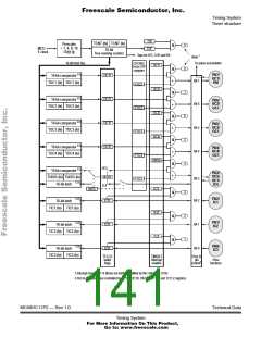
Freescale Semiconductor, Inc.
Timing System
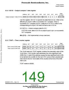
Output compare
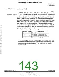
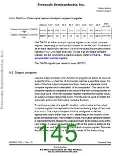
8.4.3 TI4/O5 — Timer input capture 4/output compare 5 register
State
on reset
Address bit 7 bit 6 bit 5 bit 4 bit 3 bit 2 bit 1 bit 0
Capture 4/compare 5 (TI4/O5)
high
$001E (bit 15) (14)
$001F (bit 7) (6)
(13)
(5)
(12)
(4)
(11)
(3)
(10)
(2)
(9) (bit 8) 1111 1111
(1) (bit 0) 1111 1111
Capture 4/compare 5 (TI4/O5)
low
Use TI4/O5 as either an input capture register or an output compare
register, depending on the function chosen for the PA3 pin. To enable it
as an input capture pin, set the I4/O5 bit in the pulse accumulator control
register (PACTL) to logic level one. To use it as an output compare
register, set the I4/O5 bit to a logic level zero. Refer to PACTL — Pulse
accumulator control register.
The TI4/O5 register pair resets to ones ($FFFF).
8.5 Output compare
Use the output compare (OC) function to program an action to occur at
a specific time — when the 16-bit counter reaches a specified value. For
each of the five output compare functions, there is a separate 16-bit
compare register and a dedicated 16-bit comparator. The value in the
compare register is compared to the value of the free-running counter on
every bus cycle. When the compare register matches the counter value,
an output compare status flag is set. The flag can be used to initiate the
automatic actions for that output compare function.
To produce a pulse of a specific duration, write a value to the output
compare register that represents the time the leading edge of the pulse
is to occur. The output compare circuit is configured to set the
appropriate output either high or low, depending on the polarity of the
pulse being produced. After a match occurs, the output compare register
is reprogrammed to change the output pin back to its inactive level at the
next match. A value representing the width of the pulse is added to the
original value, and then written to the output compare register. Because
the pin state changes occur at specific values of the free-running
MC68HC11P2 — Rev 1.0
Technical Data
Timing System
For More Information On This Product,
Go to: www.freescale.com

 FREESCALE [ Freescale ]