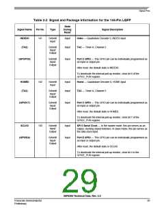
Signal Pins
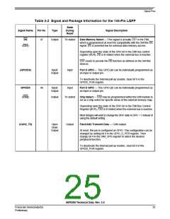
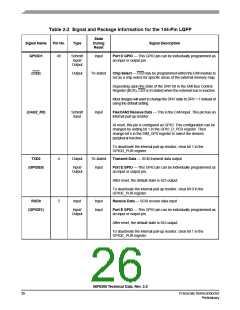
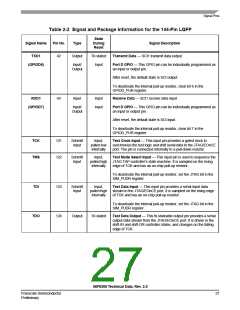
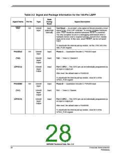
Table 2-2 Signal and Package Information for the 144-Pin LQFP
State
Signal Name
Pin No.
Type
During
Reset
Signal Description
DS
47
Output
Tri-stated
Data Memory Select — This signal is actually CS1 in the EMI,
which is programmed at reset for compatibility with the 56F80x DS
signal. DS is asserted low for external data memory access.
(CS1)
Depending upon the state of the DRV bit in the EMI bus control
register (BCR), DS is tri-stated when the external bus is inactive.
CS1 resets to provide the DS function as defined on the 56F80x
devices.
(GPIOD9)
Input/
Input
Port D GPIO — This GPIO pin can be individually programmed as
Output
an input or output pin.
To deactivate the Internal pull-up resistor, clear bit 9 in the
GPIOD_PUR register.
GPIOD0
(CS2)
48
Input/
Output
Input
Port D GPIO — This GPIO pin can be individually programmed as
an input or output pin.
Output
Tri-stated
Chip Select — CS2 may be programmed within the EMI module to
act as a chip select for specific areas of the external memory map.
Depending upon the state of the DRV bit in the EMI Bus Control
Register (BCR), CS2 is tri-stated when the external bus is inactive.
Most designs will want to change the DRV state to DRV = 1 instead of
using the default setting.
(CAN2_TX)
Open
Drain
Output
FlexCAN2 Transmit Data — CAN output.
Output
At reset, this pin is configured as GPIO. This configuration can be
changed by setting bit 0 in the GPIO_D_PER register. Then
change bit 4 in the SIM_GPS register to select the desired
peripheral function.
To deactivate the internal pull-up resistor, clear bit 0 in the
GPIOD_PUR register.
56F8366 Technical Data, Rev. 2.0
Freescale Semiconductor
Preliminary
25

 FREESCALE [ Freescale ]