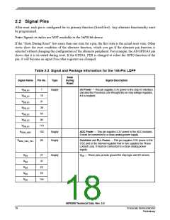
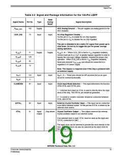
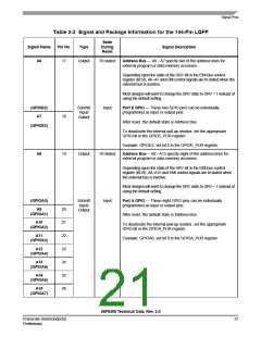
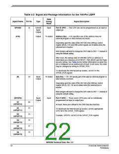
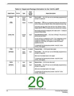
Table 2-2 Signal and Package Information for the 144-Pin LQFP
State
Signal Name
GPIOB0
Pin No.
Type
During
Reset
Signal Description
33
Schmitt
Input/
Input
Port B GPIO — This GPIO pin can be programmed as an input or
output pin.
Output
(A16)
Output
Tri-stated
Address Bus — A16 specifies one of the address lines for
external program or data memory accesses.
Depending upon the state of the DRV bit in the EMI bus control
register (BCR), A16 and EMI control signals are tri-stated when the
external bus is inactive.
Most designs will want to change the DRV state to DRV = 1 instead of
using the default setting.
After reset, the startup state of GPIOB0 (GPIO or address) is
determined as a function of EXTBOOT, EMI_MODE and the Flash
security setting. See Table 4-4 for further information on when this
pin is configured as an address pin at reset. In all cases, this state
may be changed by writing to GPIOB_PER.
To deactivate the internal pull-up resistor, set bit 0 in the
GPIOB_PUR register.
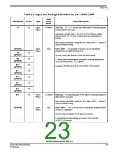
D0
59
Input/
Tri-stated
Data Bus — D0 - D6 specify part of the data for external program or
Output
data memory accesses.
Depending upon the state of the DRV bit in the EMI bus control
register (BCR), D0 - D6 are tri-stated when the external bus is
inactive.
Most designs will want to change the DRV state to DRV = 1 instead of
using the default setting.
(GPIOF9)
Input/
Input
Port F GPIO — These seven GPIO pins can be individually
Output
programmed as input or output pins.
D1
(GPIOF10)
60
72
75
76
77
78
At reset, these pins default to the EMI Data Bus function.
D2
(GPIOF11)
To deactivate the internal pull-up resistor, set the appropriate
GPIO bit in the GPIOF_PUR register.
D3
(GPIOF12)
Example: GPIOF9, set bit 9 in the GPIOF_PUR register.
D4
(GPIOF13)
D5
(GPIOF14)
D6
(GPIOF15)
56F8366 Technical Data, Rev. 2.0
22
Freescale Semiconductor
Preliminary

 FREESCALE [ Freescale ]