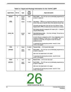
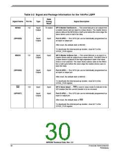
Table 2-2 Signal and Package Information for the 144-Pin LQFP
State
Signal Name
GPIOD1
Pin No.
Type
During
Reset
Signal Description
49
Schmitt
Input/
Input
Port D GPIO — This GPIO pin can be individually programmed as
an input or output pin.
Output
(CS3)
Output
Tri-stated
Chip Select — CS3 may be programmed within the EMI module to
act as a chip select for specific areas of the external memory map.
Depending upon the state of the DRV bit in the EMI Bus Control
Register (BCR), CS3 is tri-stated when the external bus is inactive.
Most designs will want to change the DRV state to DRV = 1 instead of
using the default setting.
(CAN2_RX)
Schmitt
Input
Input
FlexCAN2 Receive Data — This is the CAN input. This pin has an
internal pull-up resistor.
At reset, this pin is configured as GPIO. This configuration can be
changed by setting bit 1 in the GPIO_D_PER register. Then
change bit 5 in the SIM_GPS register to select the desired
peripheral function.
To deactivate the internal pull-up resistor, clear bit 1 in the
GPIOD_PUR register.
TXD0
4
Output
Tri-stated
Input
Transmit Data — SCI0 transmit data output
(GPIOE0)
Input/
Port E GPIO — This GPIO pin can be individually programmed as
Output
an input or output pin.
After reset, the default state is SCI output.
To deactivate the internal pull-up resistor, clear bit 0 in the
GPIOE_PUR register.
RXD0
5
Input
Input
Input
Receive Data — SCI0 receive data input
(GPIOE1)
Input/
Port E GPIO — This GPIO pin can be individually programmed as
Output
an input or output pin.
After reset, the default state is SCI output.
To deactivate the internal pull-up resistor, clear bit 1 in the
GPIOE_PUR register.
56F8366 Technical Data, Rev. 2.0
26
Freescale Semiconductor
Preliminary

 FREESCALE [ Freescale ]