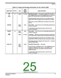
Signal Pins
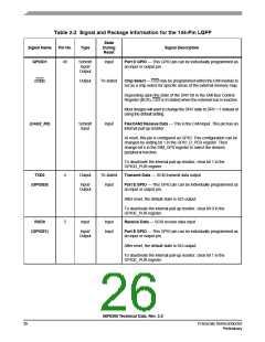
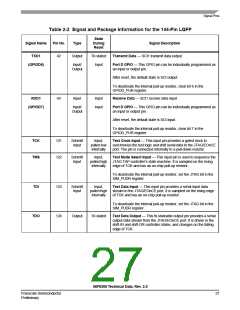
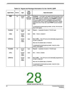
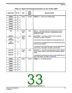
Table 2-2 Signal and Package Information for the 144-Pin LQFP
State
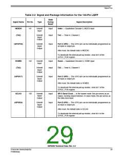
Signal Name
INDEX0
Pin No.
Type
During
Reset
Signal Description
Index — Quadrature Decoder 0, INDEX input
TA2 — Timer A, Channel 2
141
Schmitt
Input
Input
Input
(TA2)
Schmitt
Input/
Output
(GPOPC6)
Schmitt
Input/
Input
Port C GPIO — This GPIO pin can be individually programmed as
an input or output pin.
Output
After reset, the default state is INDEX0.
To deactivate the internal pull-up resistor, clear bit 6 of the
GPIOC_PUR register.
HOME0
(TA3)
142
Schmitt
Input
Input
Input
Home — Quadrature Decoder 0, HOME input
Schmitt
Input/
TA3 — Timer A, Channel 3
Output
(GPIOC7)
Schmitt
Input/
Input
Port C GPIO — This GPIO pin can be individually programmed as
an input or output pin.
Output
After reset, the default state is HOME0.
To deactivate the internal pull-up resistor, clear bit 7 of the
GPIOC_PUR register.
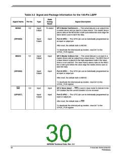
SCLK0
130
Schmitt
Input/
Output
Input
Input
SPI 0 Serial Clock — In the master mode, this pin serves as an
output, clocking slaved listeners. In slave mode, this pin serves as
the data clock input.
(GPIOE4)
Schmitt
Input/
Port E GPIO — This GPIO pin can be individually programmed as
an input or output pin.
Output
After reset, the default state is SCLK0.
To deactivate the internal pull-up resistor, clear bit 4 in the
GPIOE_PUR register.
56F8366 Technical Data, Rev. 2.0
Freescale Semiconductor
Preliminary
29

 FREESCALE [ Freescale ]