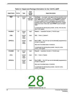
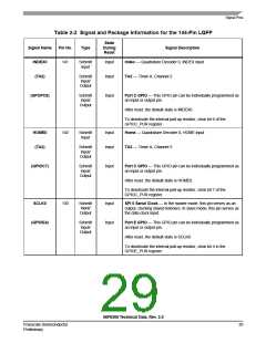
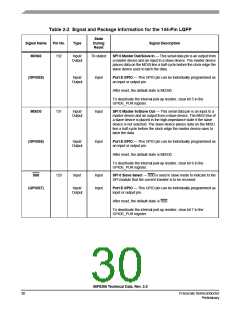
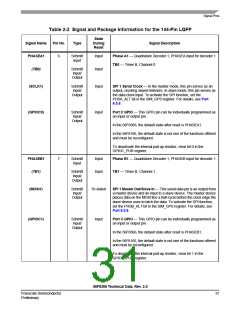
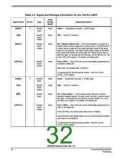
Table 2-2 Signal and Package Information for the 144-Pin LQFP
State
Signal Name
TRST
Pin No.
Type
During
Reset
Signal Description
120
Schmitt
Input
Input,
pulled high
internally
Test Reset — As an input, a low signal on this pin provides a reset
signal to the JTAG TAP controller. To ensure complete hardware
reset, TRST should be asserted whenever RESET is asserted.
The only exception occurs in a debugging environment when a
hardware device reset is required and the JTAG/EOnCE module
must not be reset. In this case, assert RESET, but do not assert
TRST.
To deactivate the internal pull-up resistor, set the JTAG bit in the
SIM_PUDR register.
PHASEA0
(TA0)
139
Schmitt
Input
Input
Input
Phase A — Quadrature Decoder 0, PHASEA input
Schmitt
Input/
TA0 — Timer A, Channel 0
Output
(GPIOC4)
Schmitt
Input/
Input
Port C GPIO — This GPIO pin can be individually programmed as
an input or output pin.
Output
After reset, the default state is PHASEA0.
To deactivate the internal pull-up resistor, clear bit 4 of the
GPIOC_PUR register.
PHASEB0
(TA1)
140
Schmitt
Input
Input
Input
Phase B — Quadrature Decoder 0, PHASEB input
Schmitt
Input/
TA1 — Timer A, Channel
Output
(GPIOC5)
Schmitt
Input/
Input
Port C GPIO — This GPIO pin can be individually programmed as
an input or output pin.
Output
After reset, the default state is PHASEB0.
To deactivate the internal pull-up resistor, clear bit 5 of the
GPIOC_PUR register.
56F8366 Technical Data, Rev. 2.0
28
Freescale Semiconductor
Preliminary

 FREESCALE [ Freescale ]