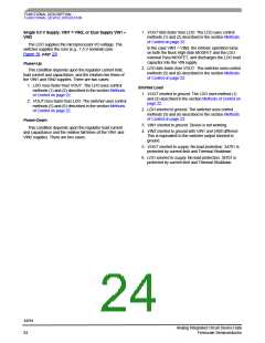
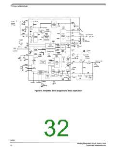
FUNCTIONAL DESCRIPTION
FUNCTIONAL DEVICE OPERATION
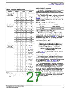
A2 A1
S
A6 A5 A4 A3
A0 0 Ack
Write
0
1
1
0 0
0
0
0
0 1 1 x x x x x
Ack
START
Slave Address
First Byte for Watchdog Programming Command Byte
0
0
1
0
0
0
0 Ack
0
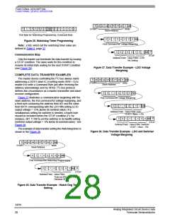
Figure 25. Watchdog Timer Programming
First Command for Voltage Margining
Note: x bits, which set the watchdog timer value are
defined in Table 8, page 27.
0
0
1
0
0
1
0
1 Ack
P
Communication Stop
STOP
Address Field Value Field = LDO
5th Setting
Only the master can terminate the data transfer by issuing
a STOP condition. The slave waits for this condition to
resume its initial state waiting for the next START condition
(see Figure 26).
Figure 27. Data Transfer Example - LDO Voltage
Margining
COMPLETE DATA TRANSFER EXAMPLES
The master device controlling the I2C bus always starts
addressing a 34701 slave IC in writing mode (R/W = 0) to
enable it to write a Command Byte just after receiving the
address acknowledge sent by 34702. I2C bus protocol
defines this circumstance as a master-transmitter and slave-
receiver configuration.
A2 A1
S
A6 A5 A4 A3
A0 0 Ack
Write
START
Slave Address
0
0
1
0
0
0
0 Ack
0
Figure 27 illustrates a communication beginning with the
slave address, the first command for voltage margining, and
a third byte containing the address field 001 and the value
field 00101 corresponding with the LDO fifth setting (LDO
output voltage = +5% above its nominal value). If a
simultaneous setting for switcher is needed, a fourth byte
should be included before the STOP condition (P); for
instance, 001 11100 to set the switcher in its twelfth setting
(switcher output voltage = -5% below its nominal value) - see
Figure 28.
First Command for Voltage Margining
0
0
1
0
0
1
0
1 Ack
Address Field Value Field: LDO
LDO = Nom. + 5%
V
0
0
1
1
1
1
0
0 Ack
P
STOP
Address Field Value Field: Switcher
OUT = Nom. - 5%
V
The example of data transfer setting the Watchdog timer is
shown in the Figure 26.
Figure 28. Data Transfer Example - LDO and Switcher
Voltage Margining
A2 A1
S
A6 A5 A4 A3
A0 0 Ack
Write
START
Slave Address
0
1
1
0
0
0
0 Ack
0
First Command for Watchdog Programming
0
1
1
0
1
0
0
1 Ack
P
STOP
Address Field Value Field:
Time-out WD = 320 ms
(Window OFF)
Figure 26. Data Transfer Example - Watch Dog Timer
Setting.
34701
Analog Integrated Circuit Device Data
Freescale Semiconductor
28

 FREESCALE [ Freescale ]