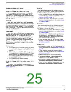
TYPICAL APPLICATION
TYPICAL APPLICATION
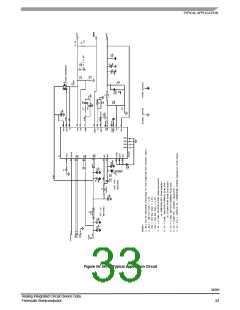
load regulation. The control circuit block diagram is shown in
Figure 29.
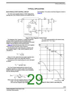
BUCK REGULATOR CONTROL CIRCUIT
The 34701 buck regulator utilizes a PWM Voltage Mode
topology with Feed-Forward to achieve an excellent line and
L
Figure 29. Buck Regulator Control Circuit
The integrated 40 pF capacitor CF charged through the
external resistor R4 provides the feed-forward ramp
waveform, the amplitude of which is proportional to the input
voltage, thus providing the feed-forward function.
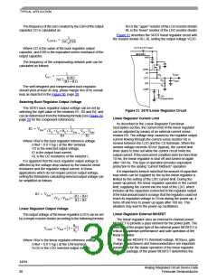
Vm1 is the ramp generated by the internal ramp
generator (Vm1 = 0.5 V typ.).
.
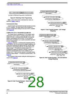
Gain
[dB]
Figure 30 shows the Bode plot of the 34701 buck regulator
control loop gain and phase versus frequency.
20
f
LC
f
z(c)
The first double pole on the Bode plot is created by the
buck regulator output L-C filter, and its frequency can be
calculated as:
f
BW
0
f
f
z(ESR) p(FF)
1
----------------------
fLC
=
f
p(c)
-20
2π COL
Where CO is the value of the buck output capacitor and L
is the inductance value of the output filter inductor L.
-40
The frequency of the compensating zero can be calculated
as follows.
-180
Phase
[Deg.]
1
----------------------------------------
fz(c)
=
2πC2(R1 + R3)
The Feed-Forward implemented by resistor R4 and
integrated capacitor CF creates a pole in the overall loop
transfer function, the frequency of which can be calculated
from the following formula.
-2 70
Φm
VIN
--------------------------------------------------------------- --------------------
1
fp(FF)
=
×
(VIN – VRef
)
2πR4CF
1
------- --------------------------------
×
+ Vm1
fsw
R4CF
-3 60
1.0
10
100
1000
10000
Where VRef is the buck regulator reference voltage
(VRef = 0.8 V typ.) at the INV terminal,
Frequency [kHz]
Figure 30. Buck Control Loop Bode Plot
VIN is the buck regulator input voltage,
34701
Analog Integrated Circuit Device Data
Freescale Semiconductor
29

 FREESCALE [ Freescale ]