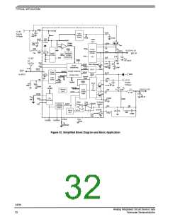
TYPICAL APPLICATION
The frequency of the zero created by the ESR of the output
capacitor CO is calculated as:
RU is the “upper” resistor of the LDO resistor divider,
RL is the “lower” resistor of the LDO resistor divider.
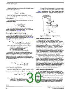
Figure 31 describes the 34701 linear regulator circuit with
the resistor divider RU, RL setting the output voltage VLDO.
1
--------------------------
fz(ESR)
=
2πCOESR
2.8 V to 6.0 V Input
Where CO is the value of the buck regulator output
capacitor, and ESR is the equivalent series resistance of the
output capacitor.
MC34701
VIN1
The frequency of the compensating network pole can be
calculated as follows:
LDRV
CS
1
V
R
LDO
S
----------------------------------------
2πC2
fp(c)
=
R1R3
LDO
LFB
-------------------------
R
C
U
LDO
(R1 + R3)
R
L
The well designed and compensated buck regulator
should yield at least 45 deg. phase margin Φm of its overall
loop as depicted in the Figure 30, page 29.
LCMP
LDO
Compensation
Selecting Buck Regulator Output Voltage
The 34701 buck regulator output voltage can be set by
selecting the right value of the resistors R1, R2 and R4, and
can be determined from the following formula (see Figure 29,
page 29 for the component references):
Figure 31. 34701Linear Regulator Circuit
Linear Regulator Current Limit
As described in the Linear Regulator Functional
1
Description section, the current limit of the linear regulator
can be adjusted by means of an external current sense
resistor RS. The voltage drop caused by the regulator output
current flowing through the current sense resistor RS is
sensed between the LDO and the CS terminals. When the
sensed voltage exceeds 50 mV (typical), the current limit
timer starts to time out while the control circuit limits the
output current. If the overcurrent condition lasts for more than
10 ms, the linear regulator is shut off and turned on again
after 100 ms. This type of operation provides equivalent
protection to the analog “current foldback” operation.
----------------------------------------------------------------------------------------
R2 = VRef
×
(V + IO × RL) – VRef
V
O – VRef
R1
--------O----------------------------------------------- -------------------------
+
R4
Where VRef is the buck regulator reference voltage
(VRef = 0.8 V typ.) at the INV terminal,
VO is the selected output voltage,
IO is the output load current,
RL is the DC resistance of the inductor L.
It is apparent that the buck regulator output voltage is
affected by the voltage drop caused by the inductor serial
resistance and the regulator output current. In those
applications which do not require precise output voltage,
setting the formula for calculating selected output voltage can
be simplified as follows:
It is important to keep in mind that the amount of capacitive
load which can be supplied by the by the linear regulator is
limited by the setting of the LDO current limit. During the
power-up period, the linear regulator operates in the current
limit, supplying the current into the load of the LDO, which
includes all the capacitors connected to the regulator output.
If the total amount load is so large that the regulator could not
reach its regulation voltage in 10 ms during the power-up, it
turns off and tries to power up again after 100 ms. This
situation may lead to the power-up oscillations.
1
--------------------------------------------------------------
R2 = VRef
×
(R1 + R4)
-------------------------
(VO – VRef) ×
R1 × R4
Linear Regulator Output Voltage
Linear Regulator External MOSFET
The output voltage of the linear regulator (LDO) can be set
by a simple resistor divider according to the following formula:
The linear regulator uses an external N-channel power
MOSFET to provide a pass element for the power path. The
selection of the proper type of the external power MOSFET is
critical for optimum performance and safe operation of the
linear regulator.
RU
⎛
⎞
⎠
-------
VLDO = VRef × 1 +
⎝
RL
The power MOSFET’s threshold voltage, RDS(on), gate
charge, capacitances and transconductance are important
parameters for the stable operation of the linear regulator
while the package of the power MOSFET determines the
Where VRef is the linear regulator reference voltage
(VRef = 0.8 V typ.) at the LFB terminal,
VLDO is the LDO selected output voltage,
34701
Analog Integrated Circuit Device Data
Freescale Semiconductor
30

 FREESCALE [ Freescale ]