FUNCTIONAL DESCRIPTION
FUNCTIONAL DEVICE OPERATION
Power-Up
INVERTED OPERATING MODE
This condition depends upon the regulator current limit,
load current and capacitance, and the relative rise times of
the VIN1 and VIN2 supplies. There are two cases:
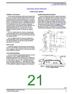
Single 3.3 V Supply, VIN = VIN1 = VIN2 = 3.3 V
The 3.3 V supplies the microprocessor I/O voltage, the
LDO supplies core voltage (e.g., 1.5 V nominal), and the
switcher VOUT operates independently. Power sequencing
depends only on the normal LDO intrinsic operation to control
the Pass MOSFET.
1. VOUT rises faster than LDO. The switcher VOUT uses
control methods (1) and (2) described in the section
Methods of Control on page 22.
2. LDO rises faster than VOUT. The LDO uses control
methods (5) and (6) described in the section Methods
of Control on page 22.
Power-Up
When VIN is rising, initially LDO is below the regulation
point and the Pass MOSFET is on. In order not to exceed the
2.1 V differential requirement between the I/O (VIN) and the
core (LDO), the LDO must start up at 2.1 V or less and be
able to maintain the 2.1 V or less differential. The maximum
slew rate for VIN is 1.0 V/ms.
Power-Down
This condition depends upon the regulator load current
and capacitance and the relative fall times of the VIN1 and
VIN2 supplies. There are two cases:
1. LDO falls faster than VOUT . The VOUT uses control
methods (4) and (5) described in the section Methods
of Control on page 22.
Power-Down
When VIN is falling, LDO falls below the regulation point;
therefore, the Pass MOSFET is on. In the case where LDO is
falling faster than VIN, the Pass MOSFET attempts to
maintain LDO. In the case where VIN is falling faster than
LDO, the Pass MOSFET is also on, and the LDO load
capacitor is discharged through the Pass MOSFET to VIN.
Thus, provided VIN does not fall too fast, the core voltage
(LDO) does not exceed the I/O voltage (VIN) by more than
maximum of 0.4 V.
In the case VIN1 = VIN2, the intrinsic operation turns
on both the Buck High-Side MOSFET and the LDO
external Pass MOSFET, and discharges the VOUT
load capacitor into the VIN supply.
2. VOUT falls faster than LDO. The LDO uses control
methods (5) and (6) described in the section Methods
of Control on page 22.
Shorted Load
Shorted Load
1. LDO shorted to ground. The VOUT uses methods (1)
and (2) described in the section Methods of Control on
page 22.
1. LDO shorted to ground. This will cause the I/O voltage
to exceed the core voltage by more than 2.1 V. No load
protection.
2. VOUT shorted to ground. The LDO uses control
methods (5) and (6) described in the section Methods
of Control on page 22.
2. VIN shorted to ground. Until the LDO load capacitance
is discharged, the core voltage exceeds the I/O voltage
by more than 0.4 V. By the intrinsic operation of the
LDO, the load capacitor is discharged rapidly through
the Pass MOSFET to VIN.
3. VIN1 shorted to ground. Device is not working.
4. VIN2 shorted to ground. This is equivalent to the
switcher VOUT output shorted to ground.
3. LDO shorted to supply. No load protection.
5. LDO shorted to supply. No load protection. 34701 is
protected by current limit and Thermal Shutdown.
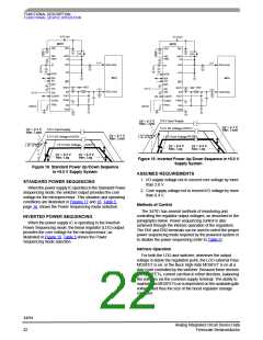
Single 5.0 V Supply, VIN1 = VIN2, or Dual Supply VIN1 ≠
6. VOUT shorted to supply. No load protection. 34701 is
VIN2
protected by current limit and Thermal Shutdown.
The switcher VOUT supplies the microprocessor I/O
voltage. The LDO supplies the core (e.g., 1.5 V nominal) (see
Figure 19, page 22).
34701
Analog Integrated Circuit Device Data
Freescale Semiconductor
25

 FREESCALE [ Freescale ]