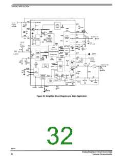
TYPICAL APPLICATION
maximum power dissipation, and hence the maximum output
current for the required input-to-output voltage drop. The
power dissipation of the external MOSFET can be calculated
from the simple formula:
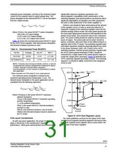
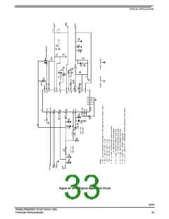
significantly improves regulation parameters and
electromagnetic compatibility (EMC) performance of the
switching regulator, poor layout practices can lead not only to
significant degradation of regulation and EMC parameters
but even to total dysfunction of the whole regulator IC.
Extreme care should be taken when laying out the ground
of the regulator circuit. In order to avoid any inductive or
capacitive coupling of the switching regulator noise into the
sensitive analog control circuits, the noisy power ground and
the clean quiet signal ground should be well separated on the
printed circuit board, and connected only at one connection
point. The power routing should be made by heavy traces or
areas of copper. The power path and its return should be
placed, if possible, atop each other on the different layers or
opposite sides of the PC board. The switching regulator input
and output capacitors should be physically placed very close
to the power terminals (VIN2, SW, PGND) of the 34701
switching regulator; and their ground terminals, together with
the 34701 power ground terminals (PGND), should be
connected by a single island of the power ground copper to
create the “single-point” grounding. Figure 32 illustrates the
34701 switching regulator grounding concept. The bootstrap
capacitor Cb should be tightly connected to the integrated
circuit as well.
PD(Q) = ILDO × (VIN – VLDO
)
Where PD(Q) is the power MOSFET power dissipation
VIN is the LDO input voltage,
VLDO is the LDO output voltage,
ILDO is the LDO output load current.
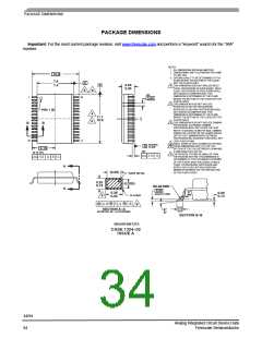
Table 10 shows the recommended power MOSFET types
for the 34701 linear regulator, their typical power dissipation,
and thermal resistance junction-to-case.
Table 10. Recommended Power MOSFETs
Part No.
Package
Typ. PD
RthJ-C
IRL2703S
D2PAK
DPAK
2.0 W
3.3 °C/W
MTD20N03HDL
1.75 W*
1.67 °C/W
NOTE: Freescale does not assume liability, endorse, or warrant
components from external manufacturers referenced in figures
or tables. Although Freescale offers component
recommendations, it is the customer’s responsibility to validate
their application.
Vin = 5.0 V
VBST
BOOT
*When mounted to an FR4 using 0.5 sq.in. drain pad size
Cb
The maximum power dissipation is limited by the
maximum operating junction temperature TJmax. The
allowed power dissipation in the given application can be
calculated from the following expression:
VIN2
SW
To L oad
Vout = 1.5 V
TJmax – TA
--------------------------------------------------------
≤
PD(Q)max
RthJC + RthCB + RthBA
INV
Vout Return
Where PD(Q)max is the power MOSFET maximum
allowed dissipation,
TJmax is the power MOSFET maximum operating
junction temperature,
TA is the ambient temperature,
PGND
GND
Power
Ground
RthJC is the power MOSFET thermal resistance
junction-to-case,
Signal
Ground
RthCB is the thermal resistance case-to-board,
RthBA is the thermal resistance board-to-ambient of
the PC board.
Figure 32. 34701 Buck Regulator Layout
PCB Layout Considerations
The same guidelines as those for the layout of the main
switching buck regulator should be applied to the layout of the
low power auxiliary boost regulator and to some extent, the
power path of the linear regulator.
As with any power application, the proper PCB layout
plays a critical role in the overall power regulator
performance. While good careful printed circuit board layout
34701
Analog Integrated Circuit Device Data
Freescale Semiconductor
31

 FREESCALE [ Freescale ]