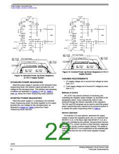
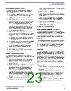
FUNCTIONAL DESCRIPTION
FUNCTIONAL DEVICE OPERATION
LOGIC COMMANDS AND REGISTERS
2
I C BUS OPERATION
Table 6. Definition of Selectable Portion of Device
Address
The 34701 device is compatible with the I2C interface
standard. SDA and SCL terminals are the Serial Data and
Serial Clock terminals of the I2C bus.
CLKSEL
Terminal
ADDR Terminal
A1
A0
2
Low
Low
0
0
1
1
0
1
0
1
I C COMMAND AND DATA FORMATS
Low
High (Open)
Low
Communication Start
High (Open)
High (Open)
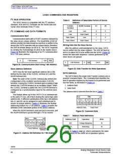
Communication starts with a START condition, followed by
the slave device unique address. The Read/Write (R/W) bit
defines whether the data should be read from or written to the
device (the 34701 operates only as a slave device; therefore,
the R/W bit should always be set to 0). The 34701 responds
by sending the Acknowledge bit (Ack) to the master device.
Figure 20 illustrates the beginning of an I2C communication
for a 7-bit slave address.
High (Open)
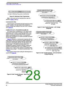
Writing Data Into the Slave Device
After the address acknowledgment by the slave, DATA
can be written into the slave registers. The R/W bit must be
set to 0 to allow DATA to be written into the 34702. Figure 22
shows the data write sequence. Actions performed by the
slave device are grayed.
Ack
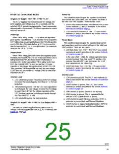
S
7-Bit Address
R/W
S
7-Bit Address
0
Ack
DATA
Ack
Figure 20. Communication Start Using 7-Bit Address
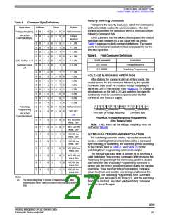
Slave Address Definition
(Write)
Figure 22. Data Transfer for Write Operations
34701 has the two least significant address bits (LSB)
defined by the state of the CLKSEL terminal (A1) and the
ADDR terminal (A0).
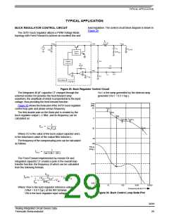
DATA Definition
The DATA field in the single Data Transfer contains one or
several Command Bytes. The Command Byte identifies the
kind of operation required by the master to be performed and
has two fields, as illustrated in Figure 23:
Note The state of the CLKSEL terminal also defines the
configuration of the oscillator synchronization CLKSYN
terminal. Leaving the CLKSEL terminal open or pulling it high
defines the CLKSYN terminal as an oscillator output. When
the CLKSEL terminal is pulled low, the CLKSYN terminal is
configured as a synchronization input for the external clock
signal.
1. Address field
2. Value field
The address field is selected from the list in Table 7.
This feature allows up to four 34701 ICs to communicate
in the same I2C bus, all of them sharing the same high-order
address bits. A different combination of the two LSB address
bits A1 and A0 can be assigned to each individual part to
assure its unique address. Figure 21 illustrates the flexible
addressing feature for a 7-bit address. Table 6 provides the
definition of the selectable portion of the device address.
MSB
7
LSB
Bits
6
5
4
3
2
1
0
D6 D5 D4 D3 D2 D1 D0
D7
Address Field
Value Field
When the ADDR terminal is used and put to low level, pull
the ADDR terminal to ground through a 10 kΩ resistor.
Figure 23. Command Byte
Table 7. Address Field Definitions
MSB
6
LSB
Bits
3
Address Field
Operation
Write
5
1
4
1
2
1
0
001
011
Voltage Margining
Watchdog
W
W
1
0
1 A1 A0
Fixed Address Selectable
Address
Refer to Table 8, page 27, which summarizes the value
field definitions for the entire set of operation options.
Figure 21. Address Bit Definition for 7-Bit Address
34701
Analog Integrated Circuit Device Data
Freescale Semiconductor
26

 FREESCALE [ Freescale ]