FUNCTIONAL DEVICE OPERATION
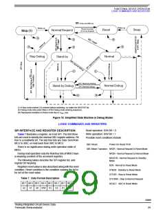
LOGIC COMMANDS AND REGISTERS
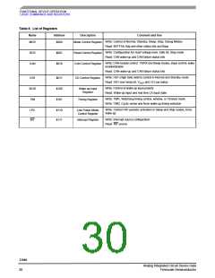
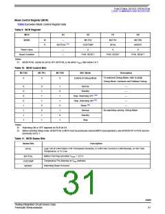
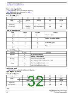
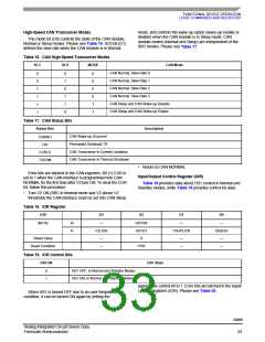
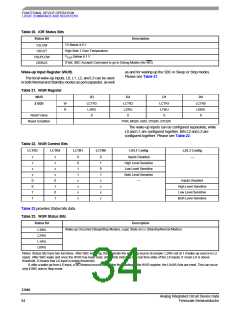
Table 8. List of Registers
Name
Address
Description
Comment and Use
Write: Control of Normal, Standby, Sleep, Stop, Debug Modes
Read: BATFAIL flag and other status bits and flags
MCR
$000
Mode Control Register
Write: Configuration for reset voltage level, Safe bit, Stop mode
Read: CAN wake-up and CAN failure status bits
RCR
CAN
$001
$010
Reset Control Register
CAN Control Register
Write: CAN module control: TX/RX and Sleep modes, slope control, wake
enable/disable
Read: CAN wake-up and CAN failure status bits
Write: HS1 (High Side switch) control in Normal and Standby mode
Read: HS1 over temp bit, VSUP and V2 Low status
IOR
WUR
TIM
$011
$100
$101
I/O Control Register
Write: Control of wake-up input polarity
Wake-up Input
Register
Read: Wake-up input and real time LX input state
Write: TIM1, Watchdog timing control, window, or Timeout mode
Write: TIM2, Cyclic sense and force wake-up timing selection
Timing Register
Write: Control HS1 periodic activation in Sleep and Stop modes, force
wake-up
LPC
INT
$110
$111
Low Power Mode
Control Register
Write: Interrupt source configuration
Read: INT source
Interrupt Register
33989
Analog Integrated Circuit Device Data
Freescale Semiconductor
30

 FREESCALE [ Freescale ]