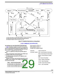
FUNCTIONAL DEVICE OPERATION
LOGIC COMMANDS AND REGISTERS
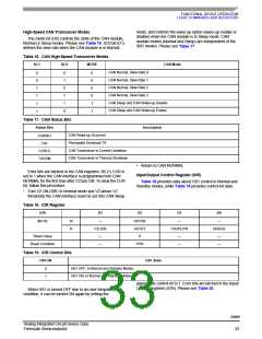
High-Speed CAN Transceiver Modes
mode, and controls the wake-up option (wake-up enable or
disable) when the CAN module is in Sleep mode. CAN
module modes (Normal and Sleep) are independent of the
SBC modes. Please see Table 17.
The mode bit (D0) controls the state of the CAN module,
Normal or Sleep modes. Please see Table 16. SC0 bit (D1)
defines the slew rate when the CAN module is in Normal
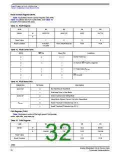
Table 16. CAN High-Speed Transceiver Modes
SC1
SC0
MODE
CAN Mode
CAN Normal, Slew Rate 0
0
0
1
1
x
x
0
1
0
1
1
0
0
0
0
0
1
1
CAN Normal, Slew Rate 1
CAN Normal, Slew Rate 2
CAN Normal, Slew Rate 3
CAN Sleep and CAN Wake-up Disable
CAN Sleep and CAN Wake-up Enable
Table 17. CAN Status Bits
Status Bits
Description
CAN Wake-up Occurred
Permanent Dominant TX
CANWU
TXF
CAN Transceiver in Current Limitation
CAN Transceiver in Thermal Shutdown
CUR(1)
THERM
• Return to CAN NORMAL
Error bits are latched in the CAN registers. Bit (1) CUR is
set to 1 when the CAN interface is programmed into CAN
NORMAL for the first time after V2 turn ON. To clear the CUR
bit, follow this procedure:
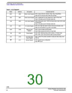
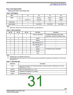
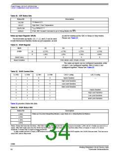
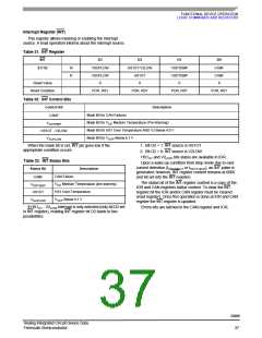
Input/Output Control Register (IOR)
Table 18 provides data about HS1 control in Normal and
Standby modes, while Table 19 provides control bit data.
• Turn V2 ON (SBC in Normal mode and V2 above V2
threshold) the CAN interface must be set into CAN Sleep
Table 18. IOR Register
IOR
D3
D2
D1
D0
$011B
W
R
—
V2LOW
—
HS1ON
HS1OT
0
—
—
DEBUG
—
VSUPLOW
Reset Value
—
—
Reset Condition
—
POR
—
Table 19. IOR Control Bits
HS1ON
HS1 State
HS1 OFF, in Normal and Standby Modes
HS1 ON, in Normal and Standby Modes
0
1
appropriate control bit to 1. Error bits are latched in the Input/
Output Registers (IOR). Please see Table 20.
When HS1 is turned OFF due to an over temperature
condition, it can be turned ON again by setting the
33989
Analog Integrated Circuit Device Data
Freescale Semiconductor
33

 FREESCALE [ Freescale ]