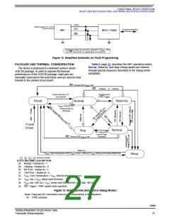
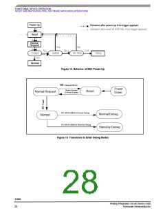
FUNCTIONAL DEVICE OPERATION
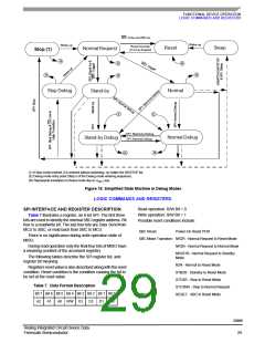
LOGIC COMMANDS AND REGISTERS
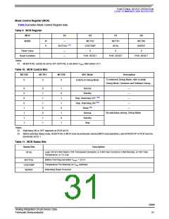
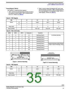
Mode Control Register (MCR)
Table 9 provides Mode Control Register data.
Table 9. MCR Register
MCR
D3
D2
D1
D0
$000B
W
R
—
MCTR2
VDDTEMP
0
MCTR1
GFAIL
MCTR0
WDRST
0
BATFAIL (31)
Reset Value
—
—
0
Reset Condition
POR, RESET
POR, RESET
POR, RESET
Notes
31. Bit BATFAIL cannot be set by SPI. BATFAIL is set when V
falls below 3.0 V.
SUP
Table 10. MCR Control Bits
MCTR2
MCTR1
MCTR0
SBC Mode
Description
To enter/exit Debug Mode, refer to detail
0
0
0
Enter/Exit Debug Mode
Debug Mode: Hardware and Software Debug...
0
0
0
0
1
1
1
1
0
1
1
1
0
0
1
1
1
0
1
1
0
1
0
1
Normal
Standby
—
—
Stop, Watchdog OFF (32)
Stop, Watchdog ON (32)
Sleep (33)
—
—
—
No watchdog running, Debug Mode
Normal
Standby
Stop
Notes
32. Watchdog ON or OFF depends on RCR bit D3.
33. Before entering Sleep mode, bit BATFAIL in MCR must be previously cleared (MCR read operation), and bit NOSTOP in RCR must be
previously set to 1.
Table 11. MCR Status Bits
Status Bits
Description
Logic OR of CAN Failure (TXF Permanent Dominant, or CAN Over Current or CAN thermal), or HS1 Over
Temperature, or V2 Low
GFAIL
Battery Fail Flag (set when V
< 3.0 V)
BATFAIL
VDDTEMP
WDRST
SUP
Temperature Pre-Warning on V
Watchdog Reset Occurred
(latched)
DD
33989
Analog Integrated Circuit Device Data
Freescale Semiconductor
31

 FREESCALE [ Freescale ]