FUNCTIONAL DEVICE OPERATION
LOGIC COMMANDS AND REGISTERS
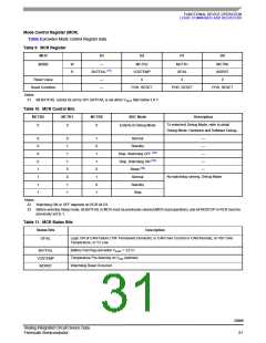
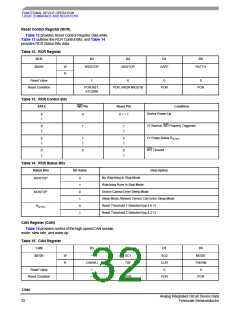
Reset Control Register (RCR)
Table 12 provides Reset Control Register data while
Table 13 outlines the RCR Control Bits, and Table 14
provides RCR Status Bits data.
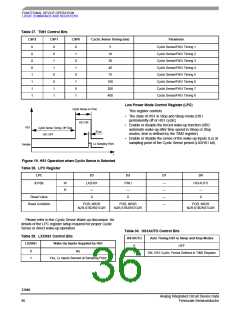
Table 12. RCR Register
RCR
D3
D2
D1
D0
$001B
W
R
WDSTOP
NOSTOP
SAFE
RSTTH
Reset Value
1
0
0
0
Reset Condition
POR,RST,
STO2NR
POR, NR2N NR2STB
POR
POR
Table 13. RCR Control Bits
SAFE
WD Pin
Reset Pin
Condition
Device Power-Up
0
1
0
0 = > 1
V1 Normal, WD Properly Triggered
0
1
1
1
1
V1 Drops Below R
STTH
0
1
1
1
0
1
WD Timeout
0
1
0
0
1
Table 14. RCR Status Bits
Status Bits
Bit Value
Description
No Watchdog in Stop Mode
WDSTOP
0
1
0
1
0
1
Watchdog Runs in Stop Mode
Device Cannot Enter Sleep Mode
NOSTOP
Sleep Mode Allowed, Device Can Enter Sleep Mode
Reset Threshold 1 Selected (typ 4.6 V)
R
STTH
Reset Threshold 2 Selected (typ 4.2 V)
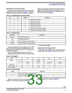
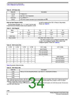
CAN Register (CAN)
Table 15 provides control of the high-speed CAN module,
mode, slew rate, and wake-up.
Table 15. CAN Register
CAN
D3
D2
D1
D0
$010B
W
R
—
CANWU
—
SC1
TXF
0
SC0
CUR
0
MODE
THERM
0
Reset Value
Reset Condition
—
POR
POR
POR
33989
Analog Integrated Circuit Device Data
Freescale Semiconductor
32

 FREESCALE [ Freescale ]