FUNCTIONAL DEVICE OPERATION
RESET AND WATCHDOG PINS, SOFTWARE WATCHDOG OPERATIONS
• Step 2–Power-up the SBC (The BATFAIL bit is set,
allowing the SBC to enter Normal Request mode)
• Step 3–Write to TIM1 register allowing SBC entering
Normal mode
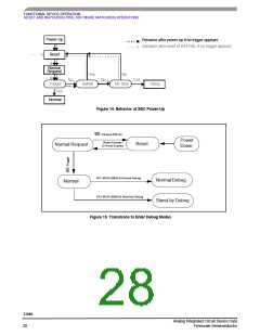
DEVICE POWER-UP, SBC WAKE-UP
After device or system power-up, or after the SBC wakes
up from Sleep mode, it enters into Reset mode prior to
moving into Normal Request mode.
• Step 4–Write to MCR register with data 0000, enabling the
Debug mode. Complete SPI byte: 000 1 0000
• Step 5–Write to MCR register normal debug (0001x101)
• Step 6–To leave the Debug mode, write 0000 to MCR
register
DEBUG MODE: HARDWARE AND SOFTWARE
DEBUG WITH THE SBC
When the SBC is mounted on the same printed circuit
board as the microcontroller it supplies, both application
software and SBC dedicated routine must be debugged. The
following features allow debug of the software by allowing the
possibility of disabling the SBC internal software Watchdog
timer.
While in Debug mode, the SBC can be used without
having to clear the WD on a regular basis to facilitate
software and hardware debug.
At Step 2, the SBC is in Normal Request. Steps 3, 4, and
5 should be completed consecutively and within the 350 ms
time period of the Normal Request mode. If this step is not
accomplished in a timely manner, the SBC will go into Reset
mode, entering Normal Request again.
DEVICE POWER-UP, RESET PIN CONNECTED TO
VDD1
At SBC power-up the VDD1 voltage is provided, but if no
SPI communication occurs to configure the device, a reset
occurs every 350 ms. In order to allow software debug and
avoid MCU reset, the Reset pin can be connected directly to
VDD1 by a jumper.
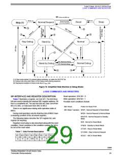
When the SBC is in Debug mode, and set in Stop Debug
or Sleep Debug, when a wake-up occurs the SBC enters
Normal Request mode for a time period of 350 ms. To avoid
the SBC generating a reset (enter Reset mode) the desired
next Debug mode (Normal Debug or Standby Debug) should
be configured within the 350 ms time period of the Normal
Request mode. For details, please refer to State Machine in
Debug mode, Figure 16.
DEBUG MODES WITH SOFTWARE WATCHDOG
DISABLED THOUGH SPI (NORMAL DEBUG,
STANDBY AND STOP DEBUG)
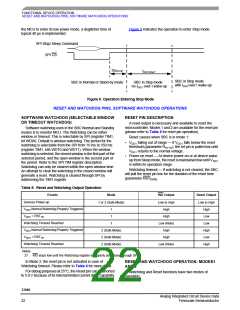
To avoid entering Debug mode after a power-up, first read
BATFAIL bit (MCR read) and write 0000 into MCR. Figure 15
illustrates the Debug mode enter.
The Watchdog software can be disabled through SPI. To
avoid unwanted watchdog disable while limiting the risk of
disabling Watchdog during SBC normal operation, the
watchdog disable must be achieved the following sequence:
• Step 1–Power down the SBC
VSUP
VDD1
Batfail
TIM1(Step 3)
MCR(Step4)
MCR (Step5)
SPI: Read Batfail
SBC in Debug Mode, No WD
Figure 11. Debug Mode Enter
MCR (Step6)
SPI
SBC Not in Debug Mode and WD ON
Debug Mode
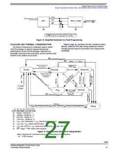
applying the correct signal to reset pins. No function of the
SBC is operating.
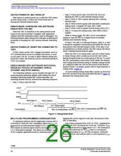
MCU FLASH PROGRAMMING CONFIGURATION
To download software into the application memory (MCU
EEPROM or Flash) the SBC capabilities allows the VDD1 to
be forced by an external power supply to 5.0 V; the reset and
WD outputs by external signal sources are forced to zero or
5.0 V, both without damage. This allows, for example, supply
of the complete application board by external power supply,
Due to pass transistor from VDD1 to VSUP, supplying the
device from VDD1 pin biases the VSUP pin. Therefore, VSUP
should not be forced to a value above 5.0 V. The Reset pin is
periodically pulled low for RSTDUR time (3.4 ms typical)
before being pulled to VDD1 for 350 ms typical. During the
time reset is low, the reset pin sinks 5.0 mA maximum (LPDW
parameter).
33989
Analog Integrated Circuit Device Data
Freescale Semiconductor
26

 FREESCALE [ Freescale ]